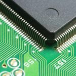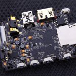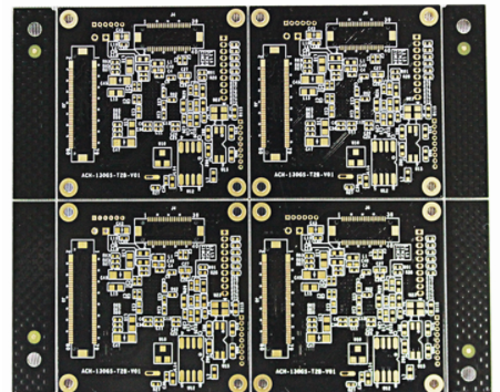
With the rapid development of electronic technology, PCB Design and PCB Manufacturing technologies continue to advance. Printed circuit boards have evolved from single-sided PCBs to double-sided and Multilayer PCBs, while the proportion of multilayer boards continues to increase across high-density electronic applications.
Modern Multilayer PCBs are developing toward higher density, finer lines, smaller features, and greater layer counts. As a result, lamination has become one of the most important processes in Multilayer PCB manufacturing. The quality of lamination directly affects interlayer bonding, dimensional stability, electrical performance, and long-term PCB reliability.
For this reason, a thorough understanding of the PCB Lamination process is essential for manufacturers and designers. Based on practical experience in multilayer board production, the following sections explain the major process considerations for improving lamination quality.
1. Design an Inner Layer Core That Meets Lamination Requirements
As lamination equipment has evolved, conventional hot pressing has increasingly been replaced by vacuum lamination technology. Modern lamination is performed in a relatively closed environment, making the preparation and design of the inner-layer stackup particularly important.
Before lamination, the Inner Layer Core should meet the following requirements.
1. Appropriate spacing between the effective panel area and the board edge
The core board should provide sufficient clearance between the effective circuit area and the outer edge of the production panel. This spacing should be optimized to minimize material waste while still providing adequate room for lamination, registration, tooling, and subsequent processing.
As a general manufacturing reference, a four-layer board may require more than 10 mm of clearance, while a six-layer board may require more than 15 mm depending on the panel structure and manufacturing process. As the layer count increases, the required working area may also increase.
The actual spacing should ultimately be determined according to the manufacturer’s PCB Manufacturing capabilities, panelization method, tooling requirements, and lamination equipment.
2. Ensure the inner core is electrically and physically qualified
Before lamination, the Inner Layer Core should be inspected to ensure that there are no open circuits, short circuits, broken traces, significant surface defects, or contamination.
The copper surface should also be clean and free from oxidation or residual film that could negatively affect resin bonding. Proper surface preparation is critical because contamination or uncontrolled surface conditions can result in poor interlayer adhesion, delamination, or reliability problems.
3. Maintain consistent core thickness and material orientation
The thickness of the core materials should be selected according to the requirements of the Multilayer PCB stackup. Core thickness should remain consistent within the specified tolerance.
For multilayer boards, especially boards with six or more layers, the orientation of the material should also be carefully controlled. Where applicable, the warp and weft directions of the laminate should be arranged consistently throughout the stackup.
Proper material orientation helps minimize mechanical stress and reduce the risk of board warpage after lamination.
4. Optimize tooling and registration hole design
Tooling-hole design is important for controlling layer-to-layer registration. A suitable number and arrangement of positioning holes can improve alignment accuracy while leaving sufficient space for production.
For example, a four-layer board may use three or more positioning holes depending on the manufacturing method. For six-layer and higher-layer-count boards, additional layer registration holes, riveting holes, and tooling holes may be required.
The exact quantity should be determined according to the manufacturer’s equipment and production method rather than using a fixed number for every design.
Tooling holes should preferably be positioned close to the panel edges while maintaining adequate clearance from the effective circuit area. This arrangement can help reduce cumulative registration errors between layers.
Target marks should also be designed to meet the recognition requirements of automated optical or tooling systems. A simple circular or concentric-circle target is commonly used because it can be identified efficiently by automated equipment.
2. Select the Appropriate Prepreg and Copper Foil Configuration
The selection of Prepreg (PP) and copper foil has a significant influence on the electrical, mechanical, and dimensional characteristics of a Multilayer PCB.
Customer requirements for prepreg may include dielectric thickness, dielectric constant, characteristic impedance, withstand voltage, resin content, bonding performance, and the surface flatness of the finished laminate.
When selecting prepreg, the following factors should be considered:
1. Ensure sufficient bonding strength and surface quality
The selected prepreg must provide adequate bonding strength between adjacent layers while maintaining the required surface quality after lamination.
2. Ensure sufficient resin flow and filling capability
During lamination, the resin must flow effectively into the spaces between printed traces and fill the required areas without creating excessive resin squeeze-out.
The appropriate prepreg type and resin content should therefore be selected according to the copper distribution, trace density, dielectric thickness, and stackup structure.
3. Meet the required dielectric thickness
The prepreg must provide the required dielectric spacing between conductive layers. This is particularly important for controlled-impedance designs, high-voltage applications, and high-speed circuits.
For high-speed PCB Design, the dielectric thickness and material properties can directly influence transmission-line impedance and signal integrity. Therefore, the prepreg selection should be evaluated together with the overall stackup design.
4. Allow adequate removal of air and volatile materials
During the Lamination Process, trapped air and volatile materials must be effectively removed. Appropriate prepreg selection and lamination conditions help reduce voids and other internal defects.
5. Select copper foil according to application requirements
Copper foil should be selected according to electrical performance, current-carrying requirements, mechanical strength, etching requirements, and customer specifications.
The copper foil grade and quality should comply with the applicable IPC requirements and the manufacturer’s process specifications.
For PCB Manufacturing, copper thickness should also be considered together with the required trace width, etching compensation, impedance requirements, plating process, and final copper thickness.
3. Inner Layer Core Surface Treatment
Before the PCB Lamination process, the inner-layer cores require appropriate surface treatment. Traditional processes may include black oxide treatment, while modern production may use alternative oxide or oxide-replacement technologies depending on the manufacturer’s process.
The purpose of this treatment is to improve the interaction between the copper surface and the resin system.
The main functions include:
1. Increase the effective bonding area
Surface treatment increases the effective contact area of the inner-layer copper, improving the mechanical bonding between copper foil and resin.
2. Improve chemical resistance
A properly treated copper surface can improve resistance during subsequent wet processes and help reduce defects such as the pink-ring phenomenon around drilled holes.
3. Improve thermal stability of the bonding interface
The treated copper surface provides a more suitable interface for the resin system during heating. This helps maintain bonding performance under the elevated temperatures encountered during the Lamination Process.
4. Improve resin wetting
As the resin melts and flows during lamination, good surface characteristics allow the resin to wet the copper surface more effectively.
The resin can then penetrate the microscopic surface structure and form a strong mechanical bond after curing.
However, surface treatment must be carefully controlled. Excessive treatment, insufficient treatment, contamination, or improper storage after treatment can all negatively affect interlayer adhesion and PCB reliability.
4. Optimize the Lamination Parameters
The control of Lamination Parameters mainly involves the coordinated management of temperature, pressure, and time.
These three parameters cannot be considered independently. Their interaction determines resin flow, wetting, curing behavior, void removal, layer registration, board thickness, and final laminate quality.
Temperature Control
Several temperature-related parameters are particularly important during PCB Lamination, including:
- Resin melting temperature
- Resin flow temperature range
- Resin curing temperature
- Hot-plate or chamber temperature
- Actual material temperature
- Heating rate
- Gel time and curing time
When the temperature reaches the resin’s softening or melting range, the resin begins to soften and flow. As the temperature increases further, resin viscosity decreases and flow capability increases.
This flow stage is essential because the resin must fill the required spaces between copper patterns and wet the copper surfaces effectively.
As the temperature continues to rise, resin flow eventually decreases as the curing reaction progresses. When the resin reaches the curing stage, its mobility becomes very low and the laminate structure begins to stabilize.
Therefore, the heating profile must be carefully controlled.
Heating rate is especially important.
If the heating rate is too fast, the resin may not have sufficient time to flow, wet the copper surfaces, and remove trapped air. Excessive resin flow can also lead to resin squeeze-out or uneven distribution.
If the heating rate is too slow, production efficiency may decrease and the resin may begin curing before it has adequately filled the required areas.
The appropriate heating rate depends on the prepreg type, resin system, resin content, copper distribution, stackup structure, and equipment characteristics.
For example, the source process reference indicates that 7628 prepreg can generally tolerate a relatively faster heating rate, while 1080 and 2116 prepregs may require more controlled heating. When a larger amount of prepreg is used, the heating rate should be carefully evaluated because excessive heating can affect resin flow and wetting behavior.
The hot-plate or chamber temperature is also important. Typical lamination systems may operate around 180–200°C, but the actual setting must follow the material supplier’s recommended curing profile and the manufacturer’s validated process window.
Pressure Control
The primary purpose of lamination pressure is to ensure that the resin fills the required spaces between layers while helping remove trapped air and volatile materials.
Different lamination presses may use different pressure profiles, including:
- Single-stage pressure
- Two-stage pressure
- Multi-stage pressure
- Vacuum-assisted pressure cycles
Conventional non-vacuum presses may use single-stage or two-stage pressure profiles, while vacuum lamination systems can use two-stage or multi-stage pressure control.
Multi-stage pressure profiles are particularly useful for high-layer-count and high-density Multilayer PCBs, where resin flow and void control become more challenging.
The required pressure should be determined according to the prepreg supplier’s recommended process window, laminate construction, resin content, board thickness, copper distribution, and press characteristics.
The source material gives a general pressure reference of approximately 15–35 kg/cm², but this should not be treated as a universal setting. Actual production parameters must be validated for the specific material system and PCB Manufacturing process.
Time Control
Time control during lamination mainly includes:
- Heating time
- Pressure application timing
- Resin flow time
- Gel time
- Main-pressure holding time
- Curing time
- Cooling time
For two-stage and multi-stage lamination, the timing of the transition from initial pressure to main pressure is particularly important.
If the main pressure is applied too early, excessive resin may be squeezed out before the resin has adequately filled the required spaces. This can result in insufficient resin content, uneven dielectric thickness, or inadequate bonding.
If the main pressure is applied too late, trapped air or volatile materials may remain inside the stackup, increasing the risk of internal voids, bubbles, or poor bonding interfaces.
Therefore, the pressure profile must be coordinated with the resin’s temperature-dependent viscosity and curing behavior.
5. Registration and Dimensional Stability During Lamination
In addition to temperature, pressure, and time, PCB Lamination must also account for dimensional changes in the laminate materials.
Copper foil, core materials, and prepreg can experience thermal expansion and contraction during heating and cooling. These changes can accumulate across multiple layers and affect layer-to-layer registration.
For high-density Multilayer PCBs, registration accuracy becomes increasingly important because fine lines, microvias, small pads, and high-density interconnect structures leave less tolerance for misalignment.
To improve registration stability, manufacturers should control:
- Core material dimensional stability
- Material orientation
- Tooling-hole accuracy
- Stackup symmetry
- Copper distribution
- Heating and cooling rates
- Press pressure profile
- Panel handling and storage conditions
A balanced stackup is particularly useful for reducing mechanical stress and minimizing board warpage.
6. Lamination Quality Inspection
After the Lamination Process, the laminated panel should be inspected before proceeding to subsequent manufacturing operations.
Important inspection items include:
- Overall board thickness
- Dielectric thickness
- Layer-to-layer registration
- Board warpage and twist
- Surface flatness
- Resin filling
- Delamination
- Internal voids
- Blisters and bonding defects
- Copper-to-resin adhesion
For demanding PCB Manufacturing applications, additional inspection methods such as cross-sectional analysis, dimensional measurement, and other reliability evaluations may be required.
Process data should also be monitored continuously so that deviations can be identified before they result in large-scale production defects.
7. Kingda’s Approach to Multilayer PCB Lamination
For manufacturers such as Kingda, controlling multilayer lamination quality requires the integration of PCB Design, material selection, stackup engineering, process control, and inspection.
A high-quality laminated board is not determined by the press cycle alone. The entire process chain must be considered, beginning with the design of the inner-layer core and continuing through prepreg selection, copper foil configuration, surface treatment, tooling, vacuum control, temperature management, pressure control, curing, cooling, and final inspection.
For customers developing high-density and high-reliability products, early communication between the PCB designer and manufacturer is also important. Stackup design, dielectric thickness, copper distribution, impedance requirements, layer registration, and material selection should be evaluated together before mass production.
This design-for-manufacturing approach helps reduce lamination-related risks and improves production consistency.
Conclusion
PCB Lamination is one of the most critical processes in Multilayer PCB manufacturing. As PCB layer counts increase and circuit structures become smaller and denser, lamination quality has an increasingly direct impact on electrical performance, dimensional accuracy, mechanical reliability, and manufacturing yield.
To achieve stable lamination results, manufacturers should carefully control the Inner Layer Core, Prepreg (PP) and copper foil configuration, surface treatment, tooling design, and key Lamination Parameters such as temperature, pressure, heating rate, and time.
At the same time, registration accuracy, resin flow, void control, dimensional stability, and post-lamination inspection should be incorporated into the overall PCB Manufacturing quality-control system.
Through systematic process optimization and close cooperation between PCB Design and manufacturing teams, companies such as Kingda can better support the production requirements of increasingly high-density, fine-feature, and high-reliability Multilayer PCBs.