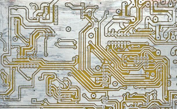
The process of transforming a copper-clad board into a functional circuit pattern is a critical stage in PCB Manufacturing. Modern circuit boards contain increasingly fine lines, smaller spacing, and more complex interconnections, making etching accuracy essential to the overall performance and reliability of the finished PCB.
One of the most widely used methods in conventional PCB Fabrication is the pattern plating process. During this process, the copper areas that need to remain on the outer layer are protected by a resist or plating layer, while the exposed unwanted copper is chemically removed through an Etching Process. The remaining copper forms the required circuit traces and conductive features.
What Is PCB Etching?
PCB Etching is a subtractive manufacturing process used to selectively remove unwanted copper from a PCB surface. After the circuit pattern has been transferred and the areas that need to remain have been protected, the exposed copper is dissolved by an appropriate chemical etchant.
The basic principle is relatively simple: the etchant reacts with exposed copper while the protected areas remain intact. However, achieving a precise circuit pattern requires careful control of chemical concentration, temperature, spray pressure, etching time, copper loading, and other process parameters.
In practical PCB Manufacturing, the objective is not simply to remove copper as quickly as possible. The etching process must remove the unwanted copper completely while minimizing undercutting beneath the resist. Excessive lateral etching can reduce the final conductor width and affect the dimensional accuracy of fine-line circuitry.
PCB Etching vs. Mechanical Routing
Chemical etching and mechanical routing are two different approaches to forming PCB circuit patterns.
Chemical PCB Etching uses an etchant to selectively dissolve exposed copper. It is widely used in conventional PCB production because it can process large areas efficiently and is suitable for high-volume manufacturing.
Mechanical routing, milling, or engraving uses a cutting tool to physically remove unwanted copper from the board surface. This method does not rely on chemical dissolution and can be useful for prototypes, laboratory development, and certain special applications.
The two methods have different advantages and limitations. Chemical etching is generally more suitable for conventional production, while mechanical routing can provide greater flexibility for rapid prototyping and small quantities.
Key Factors Affecting PCB Etching
Several factors influence the quality, dimensional accuracy, and consistency of the Etching Process.
1. Type and Chemistry of the Etchant
Different etchants have different chemical compositions and reaction characteristics. Common industrial systems include cupric chloride, ferric chloride, and alkaline etching systems.
The choice of etchant affects the etching rate, selectivity, side etching, copper loading capacity, and process stability. Therefore, the chemical system must be selected according to the PCB material, copper thickness, circuit geometry, and production requirements.
In modern PCB Manufacturing, etchant chemistry is continuously monitored and replenished to maintain stable process conditions.
2. Etching Method
The way the etchant contacts the PCB surface has a significant influence on etching uniformity.
Traditional immersion methods can provide relatively simple processing but may result in less uniform chemical exchange across the board. Spray etching systems continuously deliver etchant to the PCB surface at controlled pressure and flow rates.
Spray etching is widely used in production because it provides more effective chemical circulation and can improve etching uniformity, particularly for boards with relatively large copper areas or fine circuit patterns.
3. Etchant Density and Copper Loading
The concentration and copper loading of the etching solution must be controlled within an appropriate process window.
When the etchant becomes excessively depleted or its chemical balance changes, the Etching Rate may decrease. This can increase the time required to remove exposed copper and may contribute to excessive undercutting.
Maintaining stable chemical composition is therefore an important part of process control. Automated chemical monitoring and replenishment can help maintain consistent etching performance during continuous production.
4. Etching Rate
The Etching Rate directly affects both production efficiency and circuit-pattern quality.
If the etching rate is too slow, the PCB may remain in the etching chamber for a longer period, increasing the possibility of lateral copper removal. If the etching rate is too high, insufficient process control may result in incomplete pattern development or excessive attack on protected areas.
The optimal etching rate depends on copper thickness, etchant chemistry, equipment configuration, temperature, spray pressure, and PCB design.
For fine-line PCB Fabrication, maintaining a stable and well-controlled etching rate is particularly important because even small dimensional deviations can affect conductor width and spacing.
5. Etchant pH
For alkaline etching systems, pH is an important process parameter.
Changes in pH can affect the chemical reaction rate and etching characteristics. If the pH moves outside the manufacturer’s specified process window, etching performance and pattern quality may become unstable.
Rather than applying one universal pH value to every production line, PCB manufacturers should control pH according to the specific etchant chemistry and equipment supplier’s process requirements.
Kingda can optimize chemical process parameters according to board structure, copper thickness, line geometry, and production requirements to maintain consistent PCB Etching quality.
6. Copper Foil Thickness
Copper thickness has a direct influence on the etching process.
Thicker copper requires more copper removal and generally requires greater process control to achieve the desired conductor geometry. Fine-line circuits typically require careful matching of copper thickness, resist thickness, exposure/development conditions, and etching parameters.
When designing high-density PCBs, the relationship between copper thickness and minimum line width should therefore be considered during both PCB design and manufacturing.
Understanding Underetching in PCB Manufacturing
One of the most important technical issues associated with PCB Etching is underetching, also called lateral etching.
Ideally, the etchant would remove only the exposed copper directly below the opening in the resist. In practice, the chemical reaction also progresses laterally beneath the edge of the protective layer.
As a result, the actual conductor width after etching may be smaller than the width defined by the original imaging process.
This effect becomes increasingly important as PCB geometries become finer. Excessive Underetching can result in:
- Reduced trace width
- Increased dimensional variation
- Reduced conductor cross-sectional area
- Changes in controlled impedance
- Potential open circuits on extremely fine traces
- Reduced manufacturing yield
For this reason, PCB manufacturers must compensate for expected etching characteristics during the imaging and process-design stages.
How to Improve PCB Etching Quality
Consistent PCB Etching requires coordinated control of several manufacturing parameters rather than relying on a single process variable.
Important measures include:
- Maintain stable etchant chemistry and concentration.
- Monitor copper loading and chemical activity.
- Control etchant temperature within the specified process window.
- Maintain consistent spray pressure and nozzle performance.
- Ensure uniform PCB transport through the etching equipment.
- Regularly inspect spray nozzles and circulation systems.
- Monitor line width and spacing after etching.
- Establish appropriate process compensation for fine-line designs.
- Use suitable resist materials and maintain consistent resist thickness.
- Perform regular process capability and quality analysis.
These controls help reduce variation and improve the consistency of the finished circuit pattern.
PCB Etching for Fine-Line and High-Density PCBs
As electronic products continue to become smaller and more highly integrated, PCB designs increasingly use fine traces, narrow spacing, high layer counts, and HDI structures.
These requirements place greater demands on PCB Manufacturing processes. Traditional etching techniques must be carefully optimized to prevent excessive lateral etching and maintain the dimensional accuracy required by advanced PCB designs.
For high-density boards, the entire imaging-to-etching sequence must be considered as an integrated process. Factors such as copper thickness, resist characteristics, exposure accuracy, development quality, etchant activity, and equipment uniformity can all influence the final circuit geometry.
Therefore, fine-line PCB production requires not only advanced equipment but also stable process control and manufacturing expertise.
The Role of PCB Etching in PCB Manufacturing
The purpose of PCB Etching is to remove unwanted copper and form the conductive pattern required by the circuit design.
A typical outer-layer manufacturing sequence may include:
Copper-Clad Laminate → Surface Preparation → Imaging → Resist Development → Copper Pattern Protection/Plating → PCB Etching → Resist Stripping → Inspection
The exact process flow varies depending on PCB type, layer structure, manufacturing technology, and surface requirements.
After etching, the PCB is inspected to verify critical dimensions, conductor integrity, shorts, opens, and other potential defects. Additional processes are then performed to complete the board, such as solder mask application, surface finishing, silkscreen printing, routing, and electrical testing.
Kingda’s Approach to PCB Etching
At Kingda, PCB Manufacturing is supported by systematic process control designed to maintain circuit-pattern accuracy and production consistency.
For different PCB structures and copper thicknesses, the appropriate Etching Process parameters can be established based on the board’s design requirements and manufacturing characteristics. Process monitoring helps control chemical conditions, equipment performance, and dimensional consistency throughout production.
For fine-line and high-density PCB applications, particular attention is given to trace geometry, copper thickness, etching uniformity, and potential Underetching. These controls help ensure that the fabricated circuit remains within the required manufacturing tolerances.
Conclusion
PCB Etching is a fundamental process in modern PCB Manufacturing and plays a critical role in determining circuit-pattern accuracy, production yield, and PCB reliability.
The quality of the Etching Process is affected by many variables, including etchant chemistry, etching method, copper loading, Etching Rate, temperature, pH, copper thickness, and equipment condition. Among these factors, controlling lateral etching or Underetching is particularly important for fine-line and high-density PCB production.
As PCB technology continues to advance toward smaller geometries and higher circuit density, precise etching control becomes increasingly important. By combining appropriate chemical systems, process monitoring, equipment maintenance, and manufacturing expertise, Kingda can provide stable and reliable PCB fabrication solutions for a wide range of applications.