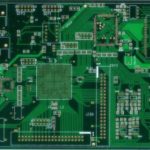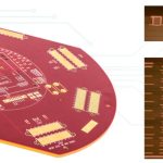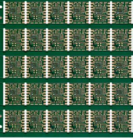
As HDI PCB technology continues to evolve alongside highly integrated ICs and high-density interconnect technology, it has become one of the most important developments in modern PCB fabrication. HDI technology enables finer lines, smaller microvias, higher wiring density, and more compact board structures, particularly for smartphones and other miniaturized electronic devices.
However, the increasing complexity of HDI structures also creates significant challenges for CAM manufacturing. Although the physical outline of an HDI smartphone PCB may appear relatively simple, its internal routing density, microvia structure, SMD arrangements, and layer-to-layer registration requirements make CAM engineering considerably more demanding than conventional PCB production.
For CAM engineers, achieving both high accuracy and fast turnaround requires a clear understanding of design data, manufacturing rules, and process limitations. Based on practical experience in PCB fabrication, this article summarizes several important CAM considerations for HDI boards.
1. Defining SMDs Correctly Is a Critical CAM Manufacturing Step
In the PCB manufacturing process, operations such as graphic data transfer, imaging, etching, solder mask processing, and plating ultimately determine whether the finished board accurately matches the customer’s design.
Therefore, during HDI PCB CAM manufacturing, CAM engineers must correctly distinguish between copper features, pads, vias, and SMDs according to the customer’s design requirements and manufacturing specifications.
Incorrect SMD definition can cause serious manufacturing problems. For example, if an SMD is defined too small or incorrectly, the actual soldering area may become insufficient, potentially resulting in defective boards or poor assembly reliability.
A typical example can be found in HDI smartphone boards using a 0.5 mm-pitch CSP. The CSP may have 0.3 mm solder pads, while some of these pads are connected directly to blind vias. If the blind via diameter is also approximately 0.3 mm, the via and CSP pad may overlap or share the same location.
This structure requires careful CAM processing because simply treating the via pad and solder pad as independent features may produce incorrect manufacturing data.
For CAM manufacturing, the following workflow can be used when processing such structures:
- Open the blind-via and buried-via structures and associate them with the corresponding drill layers.
- Define the required SMD features according to the customer’s assembly and fabrication requirements.
- Use the feature-filter and reference-selection functions in CAM software to identify pads containing blind vias on the top and bottom layers. Separate the relevant features from other copper elements.
- On the layer containing the CSP pads, identify and remove duplicate or conflicting pads associated with blind vias. Then reconstruct the CSP solder-pad pattern according to the customer’s specified pad size, pitch, position, and quantity.
- Define the reconstructed CSP as an SMD structure and correctly output the corresponding solder-mask and copper features.
- Repeat the same process for the opposite side when required.
- Finally, review the remaining undefined or incorrectly defined SMD features according to the customer’s requirements.
This approach can significantly reduce unnecessary operations compared with less structured CAM methods. More importantly, it helps minimize operator errors and improves both HDI PCB manufacturing accuracy and CAM processing efficiency.
2. Removing Non-Functional Pads in HDI PCB Manufacturing
Removing non-functional pads is another important process when preparing HDI boards for fabrication.
For example, consider a conventional eight-layer HDI structure. Non-functional pads associated with through-hole vias on layers 2–7 may need to be removed. Likewise, non-functional pads around buried-via structures between layers 3–6 may also need to be eliminated when they do not contribute to electrical connectivity.
A typical processing method includes:
- Use the CAM software’s non-functional pad removal function to identify non-plated or non-functional pads associated with the corresponding through-hole structures.
- Open all relevant drill layers except the through-hole drill layer. Set the removal option so that only unnecessary non-functional pads are removed, while electrically required pads are retained.
- For buried-via structures between layers 2 and 7, open the relevant drill layers and remove unnecessary non-functional pads from layers 3–6.
The advantage of this method is its clear processing logic. It allows CAM engineers to identify which pads are electrically required and which pads provide no functional benefit.
For engineers who are new to CAM manufacturing, establishing a consistent rule for non-functional pad removal can make HDI data preparation easier to understand and reduce the risk of accidentally removing functional copper features.
3. Laser Drilling for HDI Microvias
Laser drilling is one of the defining technologies used in HDI PCB production.
Blind microvias on HDI smartphone boards are commonly very small, often around 0.1 mm in diameter. CO₂ laser drilling is widely used for forming microvias in dielectric materials because organic dielectric materials absorb infrared laser energy efficiently.
During laser drilling, the dielectric material is rapidly heated and ablated. Copper, however, has significantly different optical and thermal characteristics and is much more difficult to remove using a conventional CO₂ laser.
For this reason, HDI manufacturing may use processes such as conformal-mask laser drilling to selectively remove dielectric material while controlling the copper structure.
From a CAM perspective, one important requirement is ensuring that sufficient copper remains at the bottom of the blind via to provide reliable interconnection.
The spacing between adjacent blind and buried vias must therefore be checked carefully. Depending on the specific material system, laser-drilling process, and manufacturer’s capabilities, the minimum spacing may need to meet strict process rules.
CAM engineers should use design-rule checks, manufacturing analysis, and drill-layer verification to determine whether the proposed via locations provide sufficient process margin.
This is especially important for high-density smartphone boards, where a small positional deviation can affect via reliability, registration accuracy, and subsequent lamination processes.
4. Via Plugging and Solder Mask Processing
Via plugging is another important consideration in HDI lamination and solder-mask manufacturing.
In many HDI stackups, RCC (Resin Coated Copper) or similar thin dielectric materials are used to achieve compact layer structures. Because the dielectric thickness and available resin content may be limited, relatively large holes or openings can create difficulties during lamination and plugging.
Based on the manufacturer’s process capability, larger non-plated holes or cavities may require dedicated plugging processes rather than relying on a single operation.
In some cases, two separate plugging steps may be required:
- The first plugging process fills the internal hole with resin and provides a relatively flat surface for subsequent lamination.
- The second plugging or solder-mask treatment is performed during the outer-layer process to prevent solder mask ink from entering or partially filling the via.
During solder-mask PCB fabrication, vias located directly on or near SMD pads can be particularly challenging.
If the customer’s requirement is to completely plug these vias, CAM engineers must carefully modify the solder-mask data. Otherwise, the via may remain partially exposed, allowing solder mask ink to leak into the hole or leaving an unintended opening after exposure.
A practical approach is to carefully control solder-mask openings around the via:
- At a via location where the solder-mask layer should remain closed, add an appropriate solder-mask feature to ensure that the via is fully covered.
- Where a controlled solder-mask opening is required, define the opening according to the customer’s specified clearance and the manufacturer’s process capability.
- Verify the final solder-mask data against the copper and drill layers to ensure that the via, pad, and SMD relationships are correct.
The exact clearance should always be determined according to the manufacturer’s process capability rather than applying a universal value to every HDI design.
5. Efficient Shape Data Preparation
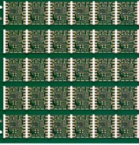
The outline of an HDI smartphone board is often supplied in a panelized format, and the customer may provide a corresponding CAD drawing.
Manually reconstructing the board outline from individual points in CAM software can be time-consuming and may introduce unnecessary errors.
A more efficient approach is to prepare the outline using the original CAD data.
For example, the CAD file can be exported into a compatible DXF format and then imported directly into the CAM system. This allows the CAM engineer to transfer the board outline, tooling holes, positioning holes, and optical targets more efficiently.
When importing the shape data, the CAM engineer should verify:
- Board outline dimensions
- Slot dimensions
- Tooling-hole locations
- Fiducial or optical-mark positions
- Panel spacing
- Datum references
- Mechanical tolerances
Directly using validated CAD geometry can improve the speed and accuracy of CAM manufacturing, particularly when processing repeated HDI panel designs.
However, imported CAD data should never be accepted without verification. The imported outline must be compared with the customer’s manufacturing drawing and checked against the actual PCB stackup and panelization requirements.
6. Milling Frame and Copper Clearance Verification
Milling-frame processing is another area that requires careful CAM inspection.
When preparing the milling frame, CAM engineers must follow both the customer’s panelization requirements and the PCB manufacturer’s manufacturing standards.
In some cases, copper may extend too close to the board edge or remain connected to the milling frame. If the remaining copper is too narrow and the two ends do not belong to the same electrical net, the milling process may unintentionally create an open circuit.
For example, if a copper connection remaining near the frame is extremely narrow, the mechanical routing process may completely cut through it.
This type of issue may not always be obvious during a conventional visual inspection. Therefore, a dedicated net comparison should be performed after frame processing.
A recommended verification procedure is:
- Compare the original copper data with the milling-frame data.
- Identify copper features that extend into the frame area.
- Simulate the required milling clearance.
- Perform a second net comparison after applying the milling operation.
- If the comparison indicates an unintended open circuit, determine whether the copper belongs to the same net or whether additional copper width is required.
- If necessary, increase the copper width or modify the milling path while maintaining the customer’s mechanical requirements.
This additional verification step can help prevent hidden manufacturing defects that may otherwise be discovered only after fabrication.
7. CAM Verification Is Essential for HDI PCB Reliability
As HDI technology continues to develop, PCB designs are becoming increasingly compact and complex. Smaller microvias, finer traces, tighter registration tolerances, and higher layer counts place greater demands on CAM manufacturing.
CAM engineering is therefore not simply a process of converting customer design files into manufacturing files. It is an engineering review process that connects PCB design requirements with actual fabrication capabilities.
For HDI PCB production, CAM engineers should pay particular attention to:
- SMD and pad definition
- Blind and buried via structures
- Non-functional pad removal
- Laser-drilling requirements
- Via plugging
- Solder-mask clearances
- Board outline and panelization
- Milling-frame design
- Layer registration
- Net connectivity
- Manufacturing tolerances
Each of these factors can influence the manufacturability, yield, electrical performance, and long-term reliability of the finished PCB.
Conclusion
The increasing adoption of HDI technology has created new opportunities for PCB miniaturization and high-density interconnection, but it has also raised the technical requirements for PCB fabrication and CAM engineering.
Accurate SMD definition, controlled removal of non-functional pads, reliable laser-drilling preparation, proper via plugging, efficient CAD data conversion, and thorough milling-frame verification are all essential parts of a robust HDI PCB CAM manufacturing workflow.
For manufacturers such as Kingda, combining advanced CAM engineering with disciplined manufacturing controls helps bridge the gap between complex HDI designs and stable mass production. By carefully reviewing design data before fabrication, CAM engineers can reduce manufacturing risks, improve production efficiency, and support the reliable production of high-density PCBs for smartphones, consumer electronics, automotive electronics, and other advanced applications.