



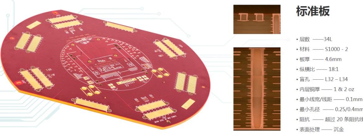
HDI PCB technology represents one of the most advanced directions in modern printed circuit board manufacturing. As electronic products continue to become smaller, lighter, and more highly integrated, conventional PCB structures are increasingly unable to meet the requirements for fine-pitch components, dense routing, and compact interconnections.
By combining finer circuit patterns, microvias, sequential lamination, and advanced plating technologies, HDI technology enables significantly higher wiring density within a smaller board area.
The core processes involved in HDI PCB manufacturing mainly include fine-line circuit fabrication, microvia formation, copper plating, and surface finishing. Each process has a direct impact on electrical performance, manufacturing yield, and long-term reliability.
This article introduces the major manufacturing processes used for HDI boards and explains the key technical considerations behind each stage.
1. Fine Circuit Fabrication
As semiconductor integration continues to increase, electronic devices are becoming increasingly compact and sophisticated. This trend places increasingly stringent requirements on PCB line width, line spacing, registration accuracy, and manufacturing consistency.
For advanced HDI applications, line width and spacing have progressed from conventional values such as 0.13 mm (5 mil) toward 0.075 mm (3 mil) and below. Some advanced manufacturing processes can achieve even finer geometries.
For HDI PCB manufacturing, forming these extremely fine circuits is one of the most technically demanding steps because even a small variation in imaging, etching, or registration can affect the final conductor geometry.
Laser Direct Imaging
One of the most important technologies used for fine circuit fabrication is laser direct imaging (LDI).
Unlike conventional photolithography, LDI uses a digitally controlled laser system to expose the required circuit pattern directly onto the photoresist-coated copper surface. This eliminates the need for conventional phototools and provides highly accurate pattern transfer.
The major advantages of LDI include:
- High pattern-transfer accuracy
- Improved registration control
- Reduced dependence on phototool alignment
- Better support for fine-line structures
- Greater flexibility for engineering changes
- Improved consistency for high-density PCB production
As circuit geometries continue to shrink, LDI has become an important imaging technology for advanced HDI PCB production.
SAP and mSAP
In addition to conventional subtractive etching, semi-additive processing (SAP) and modified semi-additive processing (mSAP) are increasingly used for high-density circuit fabrication.
In the mSAP process, a relatively thin copper layer is used as the starting material. After resist patterning, copper is selectively plated into the exposed areas to form the desired circuit pattern. The remaining seed copper is then removed or etched back.
Compared with conventional subtractive processing, SAP and mSAP provide better control over conductor geometry and are particularly suitable for fine-line applications.
These technologies have become increasingly important in applications such as smartphones, high-density modules, advanced semiconductor packages, and other compact electronic products.
2. Microvia Formation and Drilling
One of the defining characteristics of an HDI PCB is the use of microvias.
Microvias are typically very small laser-formed vias used to establish electrical connections between adjacent or nearby conductive layers. A commonly encountered microvia diameter is approximately 0.10 mm, although actual dimensions depend on the design and manufacturer’s process capability.
Microvias can be formed using either laser drilling or mechanical drilling, depending on the structure, material, and hole dimensions.
Laser Drilling
Laser drilling is widely used for HDI microvia fabrication because it can produce very small holes with high positional accuracy.
CO₂ lasers are commonly used to ablate organic dielectric materials, while UV lasers can provide finer feature control for certain applications.
The selection of laser type depends on factors such as:
- Dielectric material
- Copper thickness
- Microvia diameter
- Required aspect ratio
- Production volume
- Registration requirements
- Target manufacturing yield
During laser drilling, process parameters such as laser energy, pulse duration, repetition rate, focus position, and scanning strategy must be carefully controlled.
Improper parameters may result in resin residue, excessive dielectric damage, copper damage, or insufficient cleaning at the bottom of the microvia.
Mechanical Drilling
Although laser drilling is widely associated with HDI manufacturing, mechanical drilling remains valuable for certain hole structures.
When drilling through glass-reinforced dielectric materials, laser ablation can be affected by the different absorption and removal rates of resin and glass fibers. In some structures, residual glass fibers or uneven hole-wall morphology may require additional process control.
Mechanical drilling can provide advantages for larger holes and certain through-hole or buried-via structures.
Therefore, modern HDI PCB manufacturing does not rely exclusively on one drilling method. Laser and mechanical drilling technologies are often selected according to the specific structure and manufacturing requirements.
3. Copper Plating and Hole Filling
Copper plating is another critical stage in HDI PCB manufacturing because reliable electrical interconnection depends on stable copper deposition inside vias and across circuit surfaces.
For high-density boards, the plating process must provide sufficient uniformity while maintaining reliable coverage in microvias and other high-aspect-ratio structures.
Key factors affecting plating performance include:
- Copper plating chemistry
- Current density
- Bath temperature
- Agitation
- Additive concentration
- Plating time
- Equipment configuration
- Surface preparation
Proper process control is essential for maintaining consistent copper thickness and preventing defects such as voids, insufficient coverage, excessive thickness variation, and poor via reliability.
Microvia Copper Filling
Copper-filled microvias are widely used in advanced HDI structures.
A controlled copper-filling process can fill the microvia while maintaining an appropriate surface copper thickness. This is particularly useful for stacked microvias and via-in-pad structures.
Sequential copper plating processes can also be used for structures with different via sizes and aspect ratios.
The objective is not simply to fill the hole completely, but to achieve a controlled and reliable copper structure with minimal surface irregularity.
This is particularly important when the filled via is subsequently used as a foundation for additional sequential buildup layers.
4. Surface Finishing
After circuit fabrication and plating, the exposed copper surfaces require an appropriate surface finish to protect the copper and provide reliable solderability or wire-bonding performance.
Common surface finishes for advanced PCBs include:
- Electroless Nickel Immersion Gold (ENIG)
- Electroless Nickel Electroless Palladium Immersion Gold (ENEPIG)
- Electroless Palladium Immersion Gold (EPIG/EPAG, depending on the process specification)
- Immersion silver
- Immersion tin
- Organic solderability preservative (OSP)
The appropriate finish depends on the application, assembly process, reliability requirements, contact requirements, and cost considerations.
ENIG
ENIG consists of an electroless nickel layer covered by an immersion gold layer.
The nickel layer provides a stable surface for the immersion-gold process and serves as a diffusion barrier, while the gold protects the underlying nickel and provides good solderability.
However, because ENIG contains a relatively thick nickel layer compared with nickel-free finishes, alternative surface treatments may be considered for certain high-frequency or fine-pitch applications.
ENEPIG
ENEPIG adds a palladium layer between the electroless nickel and immersion gold layers.
The palladium layer can improve compatibility with applications requiring both soldering and wire bonding, making ENEPIG suitable for demanding electronic packages.
However, the additional process steps and material cost may make ENEPIG less attractive for applications where its additional performance is unnecessary.
Nickel-Free Surface Finishes
For some fine-line and high-frequency applications, nickel-free finishes can be considered.
Nickel-free electroless palladium/immersion gold systems can reduce the influence of the nickel layer and may provide advantages for certain high-frequency signal structures and fine-pitch applications.
The surface finish should therefore be selected based on the complete application rather than simply choosing the most advanced available coating.
5. Manufacturing Challenges for High-Density HDI PCBs
As HDI structures become more sophisticated, manufacturing challenges increasingly extend beyond individual processes.
The major challenges include:
Fine-line accuracy:
Smaller line widths and spaces require tighter control of imaging, plating, etching, and dimensional compensation.
Layer-to-layer registration:
Sequential lamination introduces multiple alignment requirements. Even small registration errors can affect microvia connections and fine-pitch pads.
Microvia reliability:
Laser-drilled microvias must have appropriate geometry, clean interfaces, and reliable copper coverage.
Copper thickness uniformity:
Uneven plating can affect impedance, current-carrying capability, etching results, and long-term reliability.
Surface finish consistency:
The surface treatment must provide stable solderability while meeting the customer’s electrical and mechanical requirements.
Process integration:
HDI manufacturing involves multiple sequential processes. A defect introduced at an early stage may not become visible until several subsequent processes have been completed.
Therefore, effective process control and inspection are essential throughout the entire production cycle.
6. The Importance of CAM and Manufacturing Engineering
Successful HDI PCB manufacturing requires close coordination between PCB design, CAM engineering, process engineering, and production.
Before manufacturing begins, CAM engineers should verify critical design parameters such as:
- Line width and spacing
- Pad dimensions
- Microvia diameter
- Via-to-pad relationships
- Layer registration
- Copper thickness
- Stack-up configuration
- Solder-mask clearances
- Surface-finish requirements
- Manufacturing tolerances
Manufacturing compensation should also be considered because actual PCB dimensions can change during imaging, etching, plating, lamination, and thermal processing.
A well-controlled CAM process can identify potential manufacturing problems before production begins, reducing rework, scrap, and delivery risk.
7. Quality Control and Reliability
The miniaturization of HDI PCB structures makes quality control increasingly important.
Depending on the application, manufacturers may use a combination of:
- Automated optical inspection (AOI)
- Automated X-ray inspection (AXI)
- Cross-sectional analysis
- Microsection inspection
- Electrical testing
- Dimensional inspection
- Plating-thickness measurement
- Surface-finish analysis
- Reliability testing
For microvia structures, cross-section analysis is particularly useful for evaluating via geometry, copper filling, interfacial quality, and potential defects.
Electrical testing is also essential to verify connectivity and identify opens, shorts, or other circuit defects.
By combining process monitoring with final inspection, manufacturers can achieve greater consistency and improve the reliability of high-density PCB production.
Conclusion
The development of HDI PCB technology has significantly expanded the possibilities of PCB miniaturization and high-density interconnection. However, achieving reliable HDI production requires precise control across every major manufacturing stage.
Fine-line circuit fabrication, laser direct imaging, mSAP, microvia drilling, copper plating, via filling, and surface finishing must work together as an integrated manufacturing system.
As electronic products continue to move toward smaller form factors and higher functional density, advanced HDI PCB manufacturing will require increasingly precise equipment, materials, process control, and engineering expertise.
Kingda continues to focus on advanced PCB manufacturing capabilities and process control, helping customers translate demanding high-density PCB designs into stable, manufacturable, and reliable products.

1 Comment
Custom Automotive LiDAR PCB Assembly for Autonomous Driving Systems | gopcba
[…] professional PCB Manufacturing, advanced assembly capabilities, and complete electronic manufacturing solutions, gopcba helps […]