High-Frequency PCB Manufacturing: Process, Materials and Key Technologies
The demand for high-performance electronic systems continues to increase as technologies such as 5G communications, radar, satellite communications, artificial intelligence, and high-speed computing become more widely adopted. In these applications, a High-Frequency PCB serves as a critical platform for transmitting and processing high-speed signals.
Unlike conventional circuit boards, high-frequency PCBs require much tighter control of dielectric properties, impedance, conductor geometry, interlayer alignment, surface quality, and manufacturing tolerances. Even small variations in materials or circuit dimensions can affect insertion loss, signal reflection, crosstalk, and overall signal integrity.
For this reason, High-Frequency PCB Manufacturing requires a carefully controlled process that begins with material selection and continues through lamination, circuit fabrication, drilling, copper plating, surface finishing, inspection, and electrical testing.
High-Frequency PCB Manufacturing Process
A reliable high-frequency PCB is produced through a series of interconnected manufacturing processes. Each stage must be controlled carefully because manufacturing variations can directly affect electrical performance at high frequencies.
1. High-Frequency PCB Material Selection
Material selection is one of the most important factors in high-frequency circuit board manufacturing.
Conventional FR-4 materials can be suitable for many electronic applications, but high-speed and RF circuits often require materials with more stable dielectric properties and lower signal losses. Common choices include PTFE-based laminates, ceramic-filled PTFE materials, high-Tg materials, and specialized high-frequency laminates.
The key material parameters include dielectric constant (Dk), dissipation factor (Df), thermal stability, dimensional stability, moisture resistance, and coefficient of thermal expansion.
For applications such as 5G and millimeter-wave communication, variations in Dk can influence signal propagation speed and impedance. A material with a stable and appropriate dielectric constant can therefore help maintain predictable electrical performance.
Copper foil is equally important. High-frequency designs may require carefully controlled copper thickness and surface characteristics because conductor roughness can contribute to signal loss, particularly as frequency increases.
For projects requiring both advanced fabrication and assembly, PCB Manufacturing can be integrated with downstream assembly requirements to improve manufacturability and production consistency. GOPCBA’s published manufacturing capabilities include multilayer, HDI, high-frequency, high-speed, rigid-flex, heavy-copper, and other advanced PCB structures.
2. Lamination Process
Lamination is a critical step in multilayer High-Frequency PCB Manufacturing.
During lamination, individual dielectric layers, copper foils, and inner circuit layers are bonded together under controlled temperature and pressure. The objective is to achieve strong interlayer bonding while maintaining accurate layer alignment and stable dielectric characteristics.
Poor lamination control can result in:
- Voids or air pockets
- Delamination
- Resin distribution problems
- Layer misalignment
- Thickness variation
- Changes in dielectric characteristics
These problems can become especially serious in high-frequency circuits because even small variations in dielectric thickness can change the impedance of controlled-impedance traces.
Advanced lamination processes therefore require accurate temperature and pressure control, appropriate material preparation, and precise registration between individual layers.
3. Circuit Formation and Etching
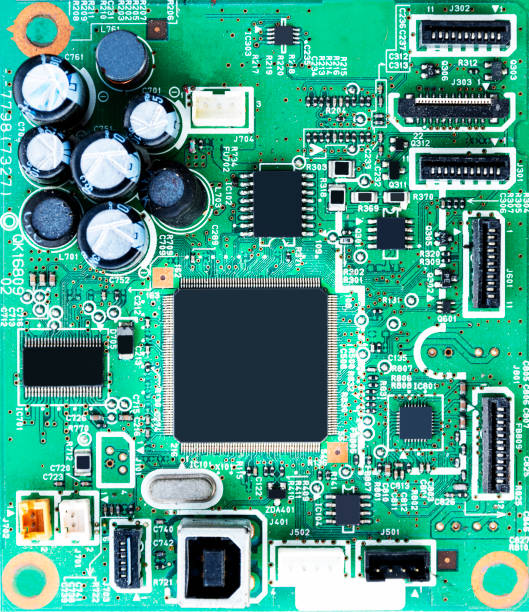
Circuit geometry has a direct influence on high-frequency signal performance.
Trace width, copper thickness, spacing, dielectric thickness, and conductor geometry all contribute to transmission-line impedance. Therefore, circuit fabrication must maintain consistent dimensions across the entire PCB.
Modern imaging technologies such as Laser Direct Imaging (LDI) can provide accurate pattern transfer for fine-line circuit structures. After imaging, the exposed circuit pattern is developed and etched to remove unwanted copper.
Etching must be carefully controlled because excessive lateral etching can reduce trace width and modify the intended impedance. Variations in conductor geometry may also increase signal reflection and loss.
For high-speed designs, the manufacturing process should therefore be optimized to maintain consistent trace dimensions rather than relying only on nominal design values.
4. Drilling and Copper Plating
Drilling creates the electrical connections between different PCB layers.
High-frequency boards may incorporate conventional through-holes, blind vias, buried vias, microvias, or other advanced interconnection structures. The selection depends on the layer stackup, routing density, signal requirements, and mechanical structure of the board.
High-precision drilling is essential because inaccurate hole positioning can affect pad registration and electrical connectivity. For small-diameter structures, laser drilling can provide the precision required for advanced PCB designs.
After drilling, the hole walls must be properly prepared before electroless copper deposition and subsequent copper plating. Uniform copper thickness is important for electrical reliability and mechanical strength.
For high-speed signal paths, unnecessary via stubs can also create discontinuities. This is one reason technologies such as back drilling are often considered for demanding high-speed designs.
5. Surface Finishing
Surface finishing protects exposed copper and provides a suitable surface for component soldering and electrical connections.
Common PCB surface finishes include:
- ENIG
- HASL
- OSP
- ENEPIG
The appropriate finish depends on the application, component package, soldering process, reliability requirements, and environmental conditions.
For high-frequency applications, surface characteristics can also influence signal performance. Therefore, the surface finish should be selected as part of the overall PCB material and manufacturing strategy rather than as an isolated production step.
Key Technologies in High-Frequency PCB Manufacturing
1. PCB Impedance Control
PCB Impedance Control is one of the most important manufacturing requirements for high-speed and RF circuit boards.
When a signal travels through a controlled-impedance transmission line, its impedance depends on several physical parameters, including:
- Trace width
- Trace thickness
- Dielectric thickness
- Dielectric constant
- Copper geometry
- Layer configuration
- Reference-plane distance
If the actual impedance differs significantly from the design target, signal reflections can occur. These reflections can reduce signal quality and potentially cause timing errors or communication failures.
A reliable impedance-control strategy therefore begins during PCB design and continues through material selection and manufacturing.
The manufacturer must maintain consistent dielectric thickness, copper thickness, trace geometry, and layer registration. Test methods such as Time Domain Reflectometry (TDR) can then be used to verify controlled-impedance structures.
This is particularly important for high-speed interfaces, RF circuits, networking equipment, and communication systems.
2. Low-Loss High-Frequency Materials
The electrical performance of a high-frequency PCB depends heavily on its dielectric material.
At higher frequencies, dielectric loss becomes increasingly important. A material with a lower dissipation factor can reduce dielectric losses and help maintain signal integrity over longer transmission distances.
Material selection should therefore consider the actual operating frequency and application environment rather than simply choosing the lowest available Dk or Df value.
For example, different materials may be appropriate for:
- 5G communication equipment
- RF modules
- Radar systems
- Satellite communication
- High-speed computing
- Automotive radar
- Industrial wireless equipment
In addition to electrical characteristics, engineers must consider thermal expansion, moisture absorption, mechanical strength, manufacturability, and compatibility with multilayer fabrication.
Advanced Technologies for High-Speed PCB Manufacturing
1. Back Drilling
Back drilling removes unused portions of plated through-holes, commonly known as via stubs.
A long via stub can behave as an unwanted transmission-line structure. At high frequencies, this can increase reflection and degrade signal integrity.
Back drilling selectively removes the unused portion of the via while retaining the required electrical connection. This approach can reduce discontinuities and improve high-speed signal performance.
It is particularly useful for high-speed digital interfaces and multilayer boards where long through-hole vias cannot otherwise be avoided.
2. Hybrid Lamination
Hybrid lamination combines different PCB laminate materials within a multilayer structure.
For example, a design may combine conventional materials with specialized high-frequency materials to balance electrical performance, thermal characteristics, mechanical requirements, and manufacturing cost.
This approach can be useful when only selected signal layers require high-frequency materials while other layers can use more economical conventional materials.
However, hybrid constructions require careful stackup engineering because different materials may have different thermal expansion characteristics, resin systems, dielectric properties, and processing requirements.
Proper material compatibility and lamination control are essential for reliable production.
3. Laser Direct Imaging
Laser Direct Imaging (LDI) is an advanced circuit imaging technology used for high-precision PCB fabrication.
Unlike conventional photographic imaging, LDI directly transfers circuit patterns onto the photoresist using a digitally controlled laser system.
Its advantages include:
- High pattern accuracy
- Improved registration
- Fine-line capability
- Better process consistency
- Reduced dependence on phototool accuracy
LDI can be particularly valuable for high-density multilayer boards, HDI structures, fine-pitch components, and high-frequency designs where trace geometry must be tightly controlled.
How Manufacturing Quality Affects High-Frequency PCB Performance
The electrical performance of a high-frequency PCB cannot be separated from its manufacturing quality.
For example, a small change in trace width can alter impedance. A variation in dielectric thickness can change transmission-line characteristics. Poor layer registration can affect differential-pair geometry. Excessive copper roughness can increase conductor loss.
Therefore, High-Speed PCB Manufacturing requires coordinated control across engineering, materials, fabrication, inspection, and testing.
A comprehensive manufacturing workflow may include:
- Engineering review
- DFM analysis
- Stackup verification
- Material preparation
- Inner-layer imaging
- Etching
- Lamination
- Drilling
- Copper plating
- Outer-layer imaging and etching
- Solder mask application
- Surface finishing
- Electrical testing
- Final inspection
Integrating engineering review with production can help identify manufacturability problems before fabrication begins. This is particularly important for complex RF, high-speed, HDI, and multilayer boards.
High-Frequency PCB Applications
High-frequency circuit boards are used in a wide range of electronic systems where signal integrity and transmission performance are critical.
Typical applications include:
5G Communication
5G base stations and RF modules require circuit boards capable of supporting high-frequency signals with controlled impedance and low transmission loss.
Radar Systems
Automotive and industrial radar systems operate at high frequencies and require precise RF signal transmission. PCB material selection, trace geometry, and manufacturing consistency are therefore critical.
Satellite and Aerospace Electronics
Satellite communication and aerospace electronics require stable electrical performance under demanding environmental conditions. High-frequency materials with appropriate thermal and mechanical properties may be required.
High-Speed Computing
Servers, networking equipment, AI hardware, and other high-performance computing systems rely on high-speed PCB structures to transmit large volumes of data.
Industrial and Medical Electronics
Specialized industrial and medical equipment may also require high-frequency PCB technologies for RF communication, sensing, imaging, and high-speed data processing.
For projects that move from engineering samples into production, Prototype PCB Assembly can help validate the PCB design and assembly process before larger production quantities are released. GOPCBA describes its prototype assembly service as covering design review, PCB manufacturing, assembly, testing, and engineering support.
Choosing a High-Frequency PCB Manufacturing Partner
Selecting a manufacturing partner for a high-frequency project involves more than comparing PCB prices.
Engineers and purchasing teams should evaluate several factors:
- High-frequency material experience
- Multilayer PCB capability
- Controlled-impedance manufacturing
- Fine-line fabrication capability
- HDI and microvia experience
- Lamination process control
- Electrical testing capability
- DFM engineering support
- Component sourcing and assembly capabilities
- Production scalability
An integrated manufacturing model can also simplify communication between PCB fabrication and assembly teams. Instead of managing PCB fabrication, component sourcing, and assembly through multiple suppliers, customers can coordinate these processes through a single manufacturing partner.
For projects requiring component sourcing as part of the manufacturing process, Components Procurement can help coordinate PCB assembly materials, availability, and production requirements. GOPCBA states that its component procurement service is integrated into its broader one-stop PCBA manufacturing model.
From Prototype to Production
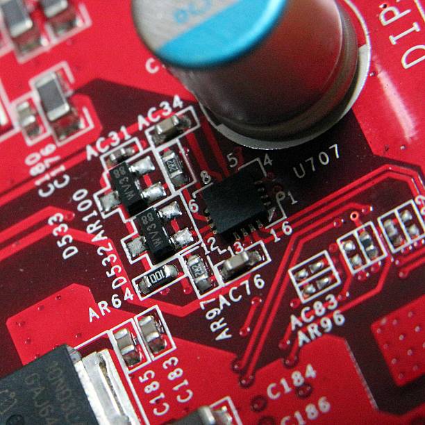
High-frequency PCB projects often evolve through several stages, from initial engineering prototypes to low-volume validation and finally volume manufacturing.
During the prototype stage, engineers can validate:
- Electrical performance
- Controlled impedance
- Signal integrity
- Thermal behavior
- Mechanical dimensions
- Component compatibility
- Assembly quality
After design validation, production quantities can be increased while maintaining the same manufacturing specifications and quality controls.
For projects requiring scalable manufacturing, High-Volume PCB Assembly can provide a transition from validated prototypes to larger production quantities. GOPCBA’s published services cover prototype, low-volume, and high-volume PCB assembly, allowing manufacturing requirements to scale with the product lifecycle.
Conclusion
High-Frequency PCB Manufacturing is a precision-driven process in which material selection, circuit geometry, lamination, drilling, copper plating, impedance control, and inspection all contribute to final electrical performance.
As electronic systems move toward higher frequencies, faster data rates, smaller form factors, and greater circuit density, traditional PCB manufacturing methods may no longer be sufficient for demanding applications.
By selecting appropriate High-Frequency PCB Materials, maintaining strict PCB Impedance Control, applying advanced fabrication technologies, and integrating engineering review with manufacturing and assembly, manufacturers can produce reliable circuit boards for 5G communications, radar, aerospace, high-speed computing, industrial electronics, and other advanced applications.
A capable manufacturing partner should therefore provide not only PCB fabrication but also engineering support, quality control, assembly, component sourcing, and scalable production. This integrated approach can reduce manufacturing risks while helping electronics companies move more efficiently from prototype development to stable production.