During PCBA Manufacturing, the PCB itself has a direct influence on the efficiency, stability, and quality of the assembly process. Although SMT placement, solder paste printing, reflow soldering, and inspection are performed on the assembly line, many potential problems originate from the PCB design or fabrication stage.
If the PCB does not meet the requirements of the assembly process, it may increase manufacturing difficulty and contribute to soldering defects, component placement problems, inspection failures, or even board rejection.
For this reason, PCB Requirements should be considered during both PCB Design and fabrication. Important factors include board dimensions, board-edge design, flatness, fiducial marks, solder-pad geometry, surface finish, and overall manufacturability.
A PCB designed with the assembly process in mind can significantly improve production efficiency and reduce unnecessary rework.
1. PCB Size
PCB Size is one of the first factors to consider when preparing a board for automated assembly.
The usable board dimensions should be compatible with the SMT line, screen printer, pick-and-place equipment, reflow oven, conveyors, and inspection systems.
As a general production reference, many assembly lines can accommodate boards within a defined size range. For example, a board with dimensions of approximately 50 mm to 460 mm may be suitable for certain production systems. However, these values are not universal industry standards and must be confirmed with the selected assembly manufacturer.
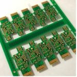
If the PCB is too small for stable transportation through the production equipment, multiple individual boards may be combined into a panel.
Panelization can improve:
- Conveyor stability
- Solder paste printing efficiency
- Component placement efficiency
- Production throughput
- Handling consistency
However, the panel design must also consider board thickness, tooling holes, fiducial marks, breakaway methods, copper distribution, and depanelization requirements.
2. PCB Edge and Board Rails
The PCB edge must provide sufficient clearance for manufacturing equipment and prevent components or solder pads from interfering with conveyors, tooling, and fixtures.
When panelization is required, the assembly panel normally includes board rails or other tooling features.
Important considerations include:
- Board-edge width
- Panel spacing
- Component-to-edge clearance
- Pad-to-edge clearance
- Depanelization method
- Conveyor support requirements
A practical starting point is to maintain adequate clearance between solder pads and the PCB edge. For example, a clearance of around 5 mm may be used in some production environments, but the exact value should be confirmed according to the assembly equipment and depanelization method.
For boards using V-groove or routed depanelization, the mechanical design should be reviewed together with the component placement.
Large components placed too close to the board edge may experience mechanical stress during depanelization or interfere with the assembly line.
3. PCB Flatness and Warpage
PCB Warpage is an important factor in automated assembly, particularly for large, thin, or multilayer boards.
Excessive warpage can affect:
- Solder paste printing
- PCB support during printing
- Component placement accuracy
- Reflow soldering
- BGA solder joint formation
- Inspection accuracy
- Depanelization
The commonly used flatness criteria depend on the applicable PCB and assembly standards, board construction, dimensions, thickness, and customer requirements.
The original production reference may specify values such as an upward bending limit of approximately 1.2 mm, a downward bending limit of approximately 0.5 mm, or a maximum deformation ratio based on the board diagonal. However, these figures should be treated as process-specific acceptance criteria rather than universal PCB standards.
For demanding applications, the manufacturer should establish the allowable warpage according to the applicable IPC requirements, assembly equipment capability, and product-specific requirements.
Major Causes of PCB Warpage
PCB warpage can result from several factors, including:
- Uneven copper distribution
- Asymmetrical multilayer stackup
- Lamination residual stress
- Different material constructions
- Thermal expansion
- Excessive thermal cycling
- Solder mask curing
- Surface finishing processes
- Mechanical processing
- Improper storage or handling
During PCB Design, balanced copper distribution and a symmetrical stackup can help reduce deformation risk.
4. Fiducial Marks
Fiducial Marks are reference features used by automated SMT equipment to accurately locate and orient the PCB or individual components.
They are particularly important for high-precision PCB Assembly involving fine-pitch components, BGA packages, QFN devices, and small passive components.
A fiducial mark is typically a small circular copper feature with a defined solder-mask clearance.
Common design considerations include:
- Circular fiducial geometry
- Appropriate fiducial diameter
- Consistent copper surface
- Flat and clean surface
- No oxidation or significant contamination
- Sufficient clearance around the mark
- High contrast between the mark and surrounding area
A typical fiducial diameter may fall within approximately 0.8–1.5 mm depending on the vision system and manufacturer requirements.
However, the exact dimensions should be confirmed with the SMT assembly provider.
Fiducial Clearance
The area surrounding the fiducial should remain free from features that could interfere with optical recognition.
Avoid placing the following too close to a fiducial:
- Vias
- Test points
- Copper patterns
- Component pads
- Silkscreen
- Solder mask features
A clear surrounding area of approximately 1 mm or more may be used as a starting point, but the actual clearance depends on the vision system.
The fiducial should also be positioned where the assembly machine can reliably recognize it. For panelized boards, both global and local fiducials may be used depending on placement accuracy requirements.
5. SMD Pad Design
SMD Pads are critical to solder paste printing and component attachment.
The pad geometry must be compatible with the component package, stencil design, solder paste volume, and reflow process.
One important principle is to avoid unnecessary through-holes inside SMD pads.
If a through-hole is placed directly in an SMD pad without an appropriate via-in-pad process, solder paste can flow into the hole during reflow. This may reduce the amount of solder available for the component termination.
Potential consequences include:
- Insufficient solder volume
- Poor solder joint formation
- Solder flowing to the opposite side
- Uneven solder distribution
- Component instability
- Reduced assembly yield
For this reason, via-in-pad structures should be intentionally designed and manufactured using an appropriate process, such as filled and capped vias, when required by the component and assembly design.
6. Pad-to-Board-Edge Clearance
The distance between a solder pad and the board edge is another important PCB Requirement.
If a pad is too close to the edge, several problems may occur:
- Difficulty supporting the PCB during printing
- Solder paste deformation
- Risk of solder bridging to adjacent structures
- Mechanical damage during depanelization
- Reduced assembly reliability
The required clearance depends on board thickness, pad geometry, component type, depanelization method, and assembly equipment.
Therefore, clearance should be specified together with the PCB manufacturer and assembly provider rather than relying on a single fixed value.
7. PCB Surface Finish
The PCB surface finish also affects solderability and assembly reliability.
Common finishes include:
- ENIG
- ENEPIG
- HASL
- Lead-free HASL
- OSP
- Immersion tin
- Immersion silver
The appropriate PCB Requirements depend on the component package, storage conditions, soldering process, reliability requirements, and product application.
For fine-pitch components and high-density assembly, a flat surface finish can be particularly beneficial because it supports more consistent solder paste deposition and component placement.
The selected surface finish should therefore be considered during PCB Design, PCB fabrication, and assembly process planning.
8. PCB Thickness and Mechanical Stability
PCB thickness affects mechanical strength, thermal behavior, and compatibility with SMT equipment.
Very thin boards may be more susceptible to:
- PCB Warpage
- Handling deformation
- Printing instability
- Placement movement
- Reflow deformation
Very thick boards may require different tooling or equipment settings.
For multilayer boards, the material stackup should also be designed to provide adequate mechanical stability.
The relationship between board thickness, copper distribution, dielectric construction, and lamination is particularly important for large-format PCBs.
9. Component-to-Edge Clearance
Components should generally be placed far enough from the board edge to avoid mechanical interference during assembly and depanelization.
This is especially important for:
- Large connectors
- BGA packages
- Tall components
- Ceramic components
- Heat sinks
- Shielding structures
- Components located near routed edges
If components must be positioned close to the edge because of product constraints, the assembly process should be reviewed in advance.
Edge clearance should therefore be treated as part of overall PCB Design for Manufacturability.
10. Design for SMT Assembly
A good PCB Assembly design should consider the complete production sequence rather than only the electrical circuit.
The PCB should be compatible with:
Solder Paste Printing → SPI → SMT Placement → Reflow Soldering → AOI → X-Ray Inspection → Testing → Depanelization
Each process places different requirements on the PCB.
For example, solder paste printing requires stable board support and accurate pad geometry. Pick-and-place requires reliable fiducial recognition and sufficient component clearance. Reflow requires appropriate thermal behavior and mechanical stability.
Therefore, electrical design and manufacturing design should be developed together.
11. Importance of Panelization
Panelization is often necessary when individual PCB dimensions are too small or when production efficiency can be improved by processing multiple boards simultaneously.
A well-designed panel should consider:
- Number of boards per panel
- Board orientation
- Board spacing
- Tooling holes
- Fiducial marks
- Board rails
- Breakaway tabs
- V-groove design
- Copper balance
- Component clearance
- Depanelization stress
The panel design should be reviewed by both the PCB fabricator and assembly manufacturer before production.
12. PCB Requirements for High-Density Components
Modern PCB Assembly increasingly uses 0201 and smaller passive components, fine-pitch ICs, BGA, QFN, LGA, and other high-density packages.
These components require tighter control of:
- Pad dimensions
- Solder mask registration
- Stencil aperture design
- Fiducial accuracy
- PCB flatness
- Surface finish
- Component placement
- Reflow profile
As component density increases, small PCB fabrication variations can have a greater influence on assembly yield.
This makes communication between the PCB manufacturer, PCB designer, and assembly provider increasingly important.
13. Common PCB Design Problems That Affect PCBA
Several PCB problems can make the assembly process more difficult.
Insufficient Board-Edge Clearance
Pads or components positioned too close to the edge may interfere with fixtures, conveyors, or depanelization.
Excessive PCB Warpage
Warped boards can reduce printing and placement accuracy and may create soldering problems during reflow.
Poor Fiducial Design
Incorrect size, insufficient clearance, contamination, or poor contrast can affect machine vision recognition.
Incorrect Pad Geometry
Improper pad dimensions can lead to insufficient or excessive solder volume and unreliable joints.
Uncontrolled Via-in-Pad Design
Unfilled vias in SMD pads can absorb solder paste and reduce solder-joint volume.
Poor Panelization
Improper board spacing, tooling, or breakaway design can increase mechanical stress and reduce production efficiency.
14. How to Improve PCB Manufacturability
To improve the transition from PCB fabrication to PCBA Manufacturing, designers should:
- Confirm PCB dimensions with the assembly manufacturer.
- Establish appropriate board-edge and component clearances.
- Control PCB Warpage according to applicable requirements.
- Use correctly designed Fiducial Marks.
- Optimize SMD Pads according to component and stencil specifications.
- Review via-in-pad requirements.
- Select an appropriate surface finish.
- Consider panelization before PCB fabrication.
- Balance copper distribution where practical.
- Confirm tooling and depanelization requirements.
- Review DFM data before production.
- Validate critical dimensions with the PCB and assembly suppliers.
Kingda’s Approach to PCB and PCBA Compatibility
At Kingda, PCB fabrication and assembly requirements are considered together to improve manufacturing compatibility.
Our engineering approach focuses on critical factors such as board dimensions, stackup, copper distribution, flatness, pad geometry, fiducial marks, surface finish, component clearance, and panelization.
For projects involving fine-pitch components or high-density assembly, additional attention can be given to fabrication tolerances and assembly-process requirements before production begins.
The objective is to identify potential manufacturing risks at the design stage rather than waiting until assembly defects occur.
Conclusion
The quality of a finished PCBA depends not only on the SMT equipment and soldering process but also on whether the PCB has been designed and manufactured for assembly.
Key PCB Requirements include appropriate PCB Size, board-edge clearance, controlled PCB Warpage, properly designed Fiducial Marks, optimized SMD Pads, suitable surface finish, and reliable panelization.
A PCB that satisfies these requirements can provide better compatibility with solder paste printing, component placement, reflow soldering, and automated inspection.
By integrating PCB Design, PCB fabrication, and PCBA Manufacturing requirements from the beginning of the project, manufacturers can reduce assembly risks, improve production efficiency, and achieve more consistent product quality.
Kingda supports customers by considering PCB manufacturability and assembly requirements throughout the production process, helping transform a reliable PCB design into a stable and production-ready PCBA.