Shenzhen PCB Prototyping: A Complete 7-Step Manufacturing Process
PCB Prototyping plays an important role in electronics development, helping engineers and manufacturers verify circuit designs before moving into larger-scale production. A reliable prototyping process must meet requirements for precision, short lead times, design flexibility, and manufacturing consistency.
A professional PCB prototyping workflow normally starts with Gerber file review and engineering verification and continues through material preparation, circuit fabrication, drilling, metallization, solder mask application, surface finishing, electrical testing, and final delivery.
For electronics companies developing new products, understanding each stage of the PCB Manufacturing process can help reduce design errors, improve prototype quality, and accelerate product development.
Step 1: PCB File Submission and Engineering Review
The first stage of PCB Prototyping is receiving and reviewing the customer’s manufacturing files. This step is critical because errors in design data can affect every subsequent manufacturing operation.
Customers typically provide Gerber files containing the required circuit layers, solder mask layers, silkscreen layers, and other manufacturing information. Drill files and special process requirements may also be required depending on the PCB structure.
Professional PCB manufacturers generally combine automated design-rule checking with manual engineering review.
File Completeness Check
Engineers first verify that all required files are available and consistent. This includes checking whether all signal layers, power layers, ground layers, solder mask layers, and silkscreen layers are included.
Drill files are also reviewed to ensure that all required hole positions and hole sizes are present. Missing or inconsistent data can result in production delays or incorrect boards.
File Format and Data Verification
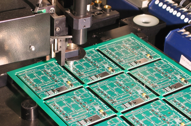
Gerber file formats, layer names, coordinates, and alignment information must be checked carefully. Consistent file structures help prevent layer misalignment, incorrect positioning, or manufacturing data incompatibility.
Manufacturing Feasibility Review
The engineering team also evaluates whether the design can be manufactured according to the required specifications.
Typical considerations include:
- Trace width and spacing
- Minimum hole diameter
- Board thickness
- Copper thickness
- Via structure
- Blind and buried vias
- Layer count
- Surface finish
- Special material requirements
If a design contains features that exceed the manufacturer’s capabilities, engineers can communicate with the customer before production begins. This helps ensure that the prototype is both manufacturable and cost-effective.
For customers who need professional assistance before manufacturing, PCB Design and Layout services can also help identify potential design-for-manufacturing issues at an early stage.
Step 2: Material Selection and Preparation
After engineering review, the next stage is selecting and preparing the PCB substrate.
Different electronic applications require different PCB materials. Material selection should consider electrical performance, thermal requirements, mechanical strength, operating environment, and overall product requirements.
For example, high-frequency applications may require materials with suitable dielectric characteristics, while high-power electronic products may benefit from substrates designed for improved thermal management.
PCB Material Cutting
The selected laminate is cut according to the required board dimensions. CNC or automated cutting equipment can be used to achieve consistent dimensions while minimizing edge damage.
During this process, manufacturers must control dimensional accuracy and prevent problems such as substrate cracking, excessive burrs, or damaged edges.
Surface Cleaning
Before circuit fabrication, the copper surface must be clean and properly prepared.
Dust, oil, oxidation, and other contaminants can negatively affect subsequent processes. Chemical cleaning or mechanical surface treatment may therefore be used to create a clean surface with suitable adhesion characteristics.
For multilayer PCB production, additional drying and preparation may be required to reduce the possibility of moisture-related problems during lamination.
Step 3: Circuit Fabrication and Pattern Transfer
Circuit fabrication is one of the most important stages of PCB Manufacturing because the quality of the copper traces directly affects the electrical performance and reliability of the finished board.
A common production method uses dry-film photoresist technology to transfer the circuit pattern onto the copper surface.
Dry Film Lamination
A photosensitive dry film is laminated onto the copper surface using controlled heat and pressure.
The dry film must be applied evenly without bubbles, wrinkles, or other defects. Proper adhesion is important because the film protects the required copper areas during the subsequent etching process.
Exposure
The circuit pattern generated from the Gerber data is transferred to the dry film using a precision exposure system.
Exposure energy and alignment accuracy must be carefully controlled. Poor exposure conditions can result in incomplete pattern transfer or dimensional deviations.
Development
After exposure, the board is processed using a developer solution.
The unexposed areas of the dry film are removed, revealing the required circuit pattern. Development time must be controlled according to the characteristics and thickness of the dry film.
Insufficient development can leave unwanted material on the board, while excessive development may affect the accuracy of the circuit pattern.
Etching
The exposed copper is processed using an etching solution to remove unwanted copper and retain the required circuit traces.
Important process parameters include etching temperature, chemical concentration, and etching speed. Proper control helps maintain trace width and improve the quality of circuit edges.
Dry Film Stripping
After etching, the remaining dry film is removed using a stripping solution. The finished copper pattern is then exposed and ready for subsequent PCB processes.
Step 4: Drilling and Metallization for Multilayer PCBs
For multilayer PCB prototypes, drilling and metallization are essential for establishing electrical connections between different circuit layers.
This stage is particularly important for boards using plated through-holes, blind vias, or buried vias.
CNC Drilling
Drilling equipment creates the required holes according to the customer’s drill files.
Different drill diameters require appropriate spindle speeds and feed rates. Accurate positioning is essential because drill deviation can affect component assembly and layer-to-layer electrical connectivity.
Manufacturers also need to control hole-wall quality and minimize problems such as burrs and resin residue.
Hole Wall Cleaning and Preparation
After drilling, the holes are cleaned to remove debris, resin residues, and other contaminants.
Micro-etching may be performed to improve the copper surface condition and promote better adhesion during subsequent metallization.
Electroless Copper Plating
A thin layer of copper is chemically deposited onto the hole walls.
This process makes the previously non-conductive hole walls electrically conductive, creating the foundation for subsequent copper electroplating.
Copper Electroplating
The copper layer is then thickened through electroplating.
Current density, plating time, chemical conditions, and other process parameters must be controlled to achieve a consistent copper thickness and reliable interlayer electrical connection.
Proper plating helps minimize defects such as uneven copper distribution, pinholes, and insufficient hole-wall coverage.
Step 5: Solder Mask and Silkscreen Application
Solder mask and silkscreen are applied after circuit fabrication and metallization.
These processes provide protection for the circuit while also adding important identification information to the PCB.
Solder Mask Application
Solder mask is applied to the PCB surface while leaving the required soldering areas exposed.
The solder mask process may include coating, pre-baking, exposure, development, and final curing.
A properly cured solder mask helps protect copper traces against moisture, dust, contamination, and accidental solder bridging during assembly.
Although green is widely used, other solder mask colors may be selected according to product requirements.
Silkscreen Printing
Silkscreen is used to print component references, polarity indicators, logos, symbols, and other identification information.
Clear and accurate silkscreen markings make component placement and PCB assembly easier, particularly during prototype development and testing.
For projects requiring a complete production solution from bare boards to assembled prototypes, Prototype PCB Assembly can be integrated into the development workflow.
Step 6: Surface Finishing and PCB Testing
Surface finishing improves the solderability and oxidation resistance of exposed copper pads.
Different surface finishes can be selected depending on PCB application, component requirements, expected storage conditions, and assembly processes.
Common PCB Surface Finishes
ENIG (Electroless Nickel Immersion Gold) uses a nickel layer and a thin gold layer to protect exposed pads. It offers good solderability and corrosion resistance and is commonly selected for applications requiring reliable and durable contact surfaces.
HASL or Tin Finishes can provide practical soldering performance and may be suitable for cost-sensitive PCB applications.
OSP (Organic Solderability Preservative) creates a protective organic coating over exposed copper surfaces. It can help prevent oxidation while maintaining good solderability for appropriate applications.
Visual Inspection
After surface finishing, boards are inspected for visible defects.
Inspection may cover:
- Circuit integrity
- Solder mask coverage
- Silkscreen clarity
- Surface finish uniformity
- Scratches or contamination
- Board appearance
Automated optical inspection (AOI) can also be used to identify certain circuit and surface defects.
Electrical Testing
Electrical testing verifies whether the PCB meets its required electrical specifications.
Depending on production requirements, manufacturers may use flying-probe testers or fixture-based testing systems to check:
- Open circuits
- Short circuits
- Electrical continuity
- Insulation resistance
- Dielectric withstand performance
For customers requiring an integrated manufacturing and assembly workflow, Turnkey PCB Assembly can combine PCB fabrication, component sourcing, and assembly services into a more streamlined process.
Dimensional Inspection
Critical physical dimensions may be checked using calipers, optical measurement equipment, or other precision inspection tools.
Typical inspection points include:
- Overall board dimensions
- Hole diameters
- Hole locations
- Trace width
- Trace spacing
- Board thickness
Additional reliability testing can be performed when required. Depending on the application, this may include high-temperature and high-humidity testing, thermal cycling, or other environmental evaluations.
Step 7: Final PCB Packaging and Delivery
Once all required inspections and tests have been completed, qualified PCB prototypes are cleaned, packaged, and prepared for shipment.
Packaging should protect the boards against moisture, contamination, mechanical damage, and electrostatic risks during transportation.
For urgent electronics development projects, efficient production scheduling and logistics coordination can significantly reduce prototype turnaround time.
A well-organized PCB Prototyping process allows manufacturers to respond quickly to design changes and engineering feedback. This is particularly valuable during product development, when engineers may need several prototype iterations before finalizing the design.
Why a Controlled PCB Prototyping Process Matters
The quality of a PCB prototype depends on more than the fabrication equipment alone. Every stage, from engineering review to final inspection, can affect the performance and reliability of the finished board.
A controlled process provides several important benefits:
Faster Design Verification
High-quality prototypes allow engineers to verify circuit performance and identify potential design problems before committing to larger production volumes.
Better Manufacturing Consistency
Standardized production procedures help maintain consistent trace dimensions, hole quality, solder mask coverage, surface finish, and electrical performance.
Reduced Production Risk
Early engineering review can identify manufacturing problems before fabrication begins, reducing the possibility of expensive rework or prototype failures.
Easier Transition to Production
A properly manufactured prototype provides a reliable reference for subsequent PCB assembly and volume manufacturing.
When projects progress beyond the prototype stage, Low Volume PCB Assembly can provide a practical bridge between engineering validation and larger production requirements.
Choosing the Right PCB Manufacturing Partner
When selecting a PCB manufacturing partner, customers should evaluate more than price and production speed.
Important factors include engineering support, manufacturing capabilities, inspection procedures, material availability, surface finishing options, assembly capabilities, and communication efficiency.
A capable supplier should be able to understand the technical requirements of the design and provide appropriate manufacturing recommendations before production begins.
For projects involving multiple manufacturing stages, integrated services can also simplify supplier management. For example, SMT PCB Assembly can be used when surface-mount components need to be assembled onto the completed PCB.
Conclusion
The Shenzhen PCB prototyping process can be divided into seven major stages: file review, material preparation, circuit fabrication, drilling and metallization, solder mask and silkscreen application, surface finishing and testing, and final delivery.
Each stage contributes to the performance, reliability, and manufacturability of the finished PCB. Careful engineering review, controlled production parameters, and comprehensive inspection are therefore essential for producing reliable prototypes.
For electronics companies developing new products, choosing an experienced manufacturing partner can help shorten development cycles, reduce manufacturing risks, and create a smoother transition from prototype validation to production.
Whether the project requires a single prototype, a small production run, or a complete PCB manufacturing and assembly solution, a well-controlled process provides the foundation for reliable electronic products.