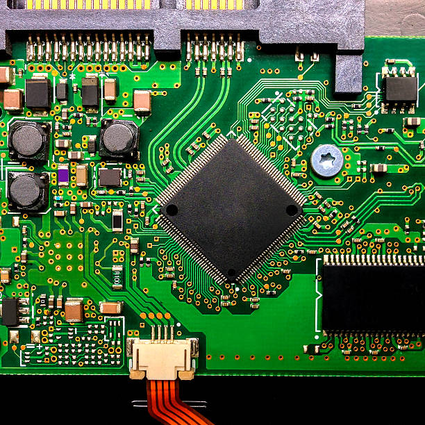
Solid-State Battery BMS Monitoring PCB: Functions, Design and Manufacturing
In a solid-state battery system, the Battery Management System (BMS) acts as the control center responsible for monitoring battery conditions, managing charging and discharging, and supporting safe operation. At the hardware level, the Solid-State Battery BMS Monitoring PCB provides the electrical platform that connects sensing circuits, control components, communication interfaces, and protection circuits.
As solid-state battery technology develops for electric vehicles, energy storage systems, industrial equipment, and other applications, the requirements for battery monitoring hardware are becoming increasingly demanding. The PCB must support accurate voltage, current, and temperature measurements while maintaining reliable signal transmission and stable operation in electrically and thermally challenging environments.
A properly designed BMS Monitoring PCB therefore plays an important role in battery safety, performance, and long-term reliability.
What Does a Solid-State Battery BMS Monitoring PCB Do?
A BMS monitoring board performs several important functions within a battery management architecture.
1. Battery Parameter Monitoring
One of the primary functions of a Battery Management System PCB is to provide reliable electrical connections between battery cells, voltage sensing circuits, temperature sensors, current sensors, and the BMS control circuitry.
The monitoring circuit continuously collects information such as:
- Individual cell voltage
- Pack voltage
- Battery current
- Cell and module temperature
- Charging and discharging conditions
- Cell voltage differences
- Abnormal operating conditions
The collected signals are transferred to the BMS controller for analysis. Accurate data acquisition is essential because incorrect measurements can lead to inappropriate charging, balancing, or protection decisions.
For battery packs containing many cells, the PCB must also support multiple sensing channels while maintaining stable signal integrity.
2. Safety Protection and Control
Battery safety is another major responsibility of the BMS.
When abnormal conditions are detected, the BMS can generate control signals for protection components such as relays, contactors, cooling systems, and charging circuits.
For example, if a temperature sensor detects an abnormal increase in battery temperature, the control system may activate cooling equipment or interrupt the charging process.
The PCB provides the electrical pathways required to transmit these signals quickly and reliably.
3. Cell Balancing and Energy Management
Battery cells may not always have identical voltage and capacity characteristics. During charging and discharging, differences between cells can gradually increase.
The BMS therefore uses balancing circuits to help maintain appropriate voltage consistency between cells.
The monitoring PCB supports this process by providing stable connections for balancing circuits and accurate voltage feedback to the main controller.
Reliable PCB design can help the BMS make better decisions regarding charging current, discharge limits, and cell balancing.
Key Performance Requirements for BMS Monitoring PCBs
The operating environment of a battery system creates several challenges for PCB design and manufacturing. A reliable BMS board should be designed around electrical accuracy, signal integrity, thermal stability, and long-term reliability.
Low Signal Interference
Voltage and temperature sensing signals can be relatively sensitive to electrical noise. Battery systems may also contain high-current conductors, switching devices, inverters, motors, and other sources of electromagnetic interference.
Poor PCB layout can allow noise from high-current or high-frequency circuits to affect sensitive analog signals.
To reduce interference, engineers should carefully separate sensitive signal traces from power traces and high-noise circuits.
Important layout considerations include:
- Analog and digital signal separation
- Appropriate grounding strategies
- Short sensing paths
- Controlled return-current paths
- Proper power and ground distribution
- Adequate spacing between high-current and low-level signals
These measures can improve measurement stability and reduce unwanted signal coupling.
Fast and Reliable Signal Transmission
A battery protection system must respond quickly when abnormal conditions occur.
The PCB should therefore minimize unnecessary signal paths and avoid layout structures that introduce excessive parasitic effects or signal degradation.
Critical protection and sensing signals should be routed according to their electrical characteristics and system requirements.
For more complex electronic products, professional PCB Manufacturing processes are important because fabrication quality can directly affect trace geometry, impedance, insulation, and overall electrical performance.
Thermal and Environmental Reliability
Battery systems may operate under elevated temperatures, vibration, humidity, and repeated thermal cycling.
The PCB materials and manufacturing processes should therefore be selected according to the actual application environment.
Important considerations include:
- Appropriate PCB substrate selection
- Thermal management
- Copper thickness
- Surface finish
- Solder mask reliability
- Insulation performance
- Mechanical strength
- Resistance to thermal cycling
For demanding applications, the PCB design should consider both electrical performance and mechanical reliability rather than focusing only on circuit functionality.
PCB Layout Considerations for Solid-State Battery BMS Applications
PCB layout is one of the most important stages in developing a BMS monitoring board.
Separate Power and Sensing Circuits
A typical BMS PCB may contain high-current paths alongside low-level voltage and temperature sensing circuits.
These circuits should not be routed without considering their potential interaction.
High-current traces can generate electromagnetic fields and voltage fluctuations that may interfere with sensitive measurement circuits.
Separating these areas and designing appropriate grounding and return paths can help improve signal quality.
Optimize Grounding
Grounding is particularly important for BMS electronics because multiple sensing channels may share common reference points.
Poor grounding can create unwanted voltage differences and measurement errors.
The PCB layout should therefore establish a well-planned grounding structure based on the circuit architecture.
Control Trace Length and Routing
Sensitive analog signals should generally use carefully planned routing paths.
Long, unnecessarily parallel traces can increase the risk of noise coupling.
Engineers should consider:
- Trace length
- Trace spacing
- Layer arrangement
- Via usage
- Ground reference
- Differential routing where appropriate
- Separation from switching nodes
These considerations become increasingly important as the number of sensing channels and circuit complexity increase.
Manufacturing Requirements for BMS Monitoring PCBs
The performance of a BMS board depends not only on circuit design but also on manufacturing quality.
A manufacturing partner should be able to maintain consistent PCB dimensions, copper features, hole quality, solder mask performance, and electrical characteristics.
Material Selection
The PCB substrate should provide appropriate:
- Electrical insulation
- Thermal stability
- Dimensional stability
- Mechanical strength
- Moisture resistance
The appropriate material depends on the battery system’s voltage, temperature, mechanical environment, and expected service life.
PCB Fabrication Accuracy
Manufacturing tolerances can affect the reliability of pads, traces, vias, connectors, and other structures.
For high-density BMS designs, accurate fabrication becomes especially important.
The PCB production process should include appropriate inspections and electrical testing to identify potential manufacturing defects before assembly.
Assembly Requirements for BMS Electronics
After PCB fabrication, electronic components must be mounted accurately and reliably.
Depending on the design, BMS boards may include:
- Microcontrollers
- Analog front-end ICs
- Battery monitoring ICs
- Temperature sensing components
- Communication components
- MOSFETs
- Relays or control interfaces
- Passive components
- Connectors
A professional PCB Assembly process helps ensure that these components are placed and soldered according to the design requirements.
For BMS applications, component placement accuracy is particularly important because sensing circuits and control circuits may have strict electrical requirements.
SMT Assembly for BMS Monitoring Boards
Many BMS monitoring PCBs use surface-mount components because SMT technology supports compact layouts and high component density.
A typical SMT production process includes:
- Solder paste printing
- Solder paste inspection
- Automated component placement
- Reflow soldering
- Automated optical inspection
- Electrical testing
- Final inspection
Fine-pitch components and compact packages require accurate placement and controlled soldering conditions.
For prototype and engineering-stage BMS projects, rapid SMT production can also help engineers validate PCB designs before moving to larger production volumes.
Prototype and Low-Volume BMS PCB Production
Battery technologies are continuously evolving, and BMS designs may require multiple engineering iterations.
Before mass production, engineers may need a limited number of prototype boards to verify:
- Cell voltage measurement
- Temperature monitoring
- Communication functions
- Protection logic
- Charging behavior
- Cell balancing
- Mechanical integration
- Firmware compatibility
For these applications, Prototype PCB Assembly can shorten the development cycle and allow engineers to identify design problems before committing to large production quantities.
Prototype manufacturing can also be useful when a BMS design includes new battery-monitoring ICs, revised sensing circuits, new communication interfaces, or a redesigned mechanical structure.
Component Procurement for BMS PCB Production
Component availability can significantly affect BMS manufacturing schedules.
A typical BMS bill of materials may include specialized ICs, precision resistors, capacitors, connectors, sensors, power devices, and communication components.
Before production, the BOM should be reviewed for:
- Manufacturer part numbers
- Component specifications
- Package types
- Availability
- Lead times
- Lifecycle status
- Approved alternatives
- Quantity requirements
Early component verification helps reduce the risk of production delays caused by unavailable or obsolete components.
For projects requiring an integrated sourcing solution, component procurement can be coordinated with PCB fabrication and assembly.
Inspection and Testing of BMS Monitoring PCBs
Quality control is essential because a PCB defect in a battery management system can potentially affect monitoring or protection functions.
Depending on the product requirements, inspection may include:
Visual Inspection
Visual inspection can identify:
- Damaged PCB surfaces
- Solder mask defects
- Pad damage
- Contamination
- Component placement problems
- Soldering abnormalities
AOI Inspection
Automated Optical Inspection can identify many assembly defects, including component placement errors, soldering problems, missing components, and polarity issues.
X-Ray Inspection
For assemblies containing hidden solder joints, such as certain BGA packages, X-ray inspection can provide additional visibility into solder connections.
Electrical Testing
Electrical tests can verify PCB continuity, insulation, and other specified electrical characteristics.
Functional Testing
Functional testing evaluates whether the assembled BMS board operates according to the customer’s requirements.
Depending on the system, functional testing may include communication, sensing, power management, protection, and control functions.
From Prototype to Production
A reliable BMS development strategy should connect engineering validation with scalable manufacturing.
A typical development workflow can be:
PCB Design → DFM Review → Prototype PCB → Component Procurement → PCB Manufacturing → PCB Assembly → Testing → Engineering Validation → Low-Volume Production → High-Volume Production
This approach allows potential design and manufacturing issues to be identified early.
An integrated manufacturing model can also reduce communication between separate PCB fabrication, component sourcing, assembly, and testing suppliers.
Why Manufacturing Integration Matters for BMS Projects
BMS electronics combine sensitive measurement circuits with power-control and communication functions. As a result, manufacturing coordination can have a significant effect on development efficiency.
An integrated supplier can coordinate:
- PCB fabrication
- Component procurement
- SMT assembly
- Through-hole assembly
- Inspection
- Electrical testing
- Functional testing
- Production scaling
This can simplify engineering communication and make it easier to manage revisions during product development.
For more complex BMS products, a Turnkey PCB Assembly model can combine material sourcing, PCB fabrication, component assembly, inspection, testing, and delivery within one coordinated manufacturing workflow.
Conclusion
The Solid-State Battery BMS Monitoring PCB is an important hardware foundation for safe and reliable battery management. It connects sensing components, control circuits, communication interfaces, and protection functions while enabling the BMS to monitor battery conditions in real time.
Successful BMS PCB development requires more than simply creating an electrically functional circuit. Engineers must consider signal integrity, electromagnetic interference, thermal conditions, grounding, trace routing, material selection, manufacturing accuracy, component placement, inspection, and functional testing.
From prototype development to production, an integrated manufacturing workflow can help reduce development risks and improve production efficiency.
For solid-state battery applications, choosing the right BMS Monitoring PCB manufacturing strategy can help create a reliable path from initial design validation to scalable production.