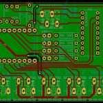
As electronic products continue to become smaller, smarter, and more highly integrated, Double-Sided PCB assembly is increasingly important in modern electronics manufacturing. Advanced products often need to accommodate a large number of components and functions within a limited space, making both sides of the circuit board available for component placement.
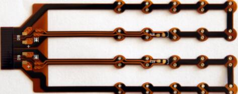
This requirement is particularly important for Rigid-Flex PCB structures. By combining the mechanical stability of rigid sections with the flexibility of flex sections, rigid-flex boards can provide significant space-saving and packaging advantages. However, using both sides of the board also introduces additional challenges to the SMT Assembly process.
For manufacturers, successful double-sided assembly requires careful consideration of component placement, solder paste printing, reflow profiles, board deformation, component weight, and overall process sequence.
Why Double-Sided SMT Assembly Is Used
Traditional single-sided assembly limits the usable area available for components. When component density increases, designers can place components on both sides of the PCB to improve space utilization and reduce the overall product footprint.
In a typical Double-Sided PCB assembly process, components are first mounted on one side of the board and then assembled on the opposite side. This allows more components to be integrated without significantly increasing the board’s length or width.
However, double-sided assembly is more complex than single-sided assembly because the board must pass through multiple printing, placement, and reflow stages.
The general process may include:
- Solder paste printing on the first side.
- Component placement on the first side.
- First reflow soldering.
- Board inspection and process verification.
- Solder paste printing on the second side.
- Component placement on the second side.
- Second reflow soldering.
- Final inspection and electrical or functional testing.
The exact sequence depends on the board structure, component types, thermal requirements, and manufacturing capabilities.
Component Placement on Both Sides of a Rigid-Flex PCB
Component placement is one of the most important factors in PCB Design for double-sided assembly.
When the first side has already been assembled, the board must be flipped before processing the second side. Components mounted on the first side will therefore face downward during the second reflow process.
This creates an important consideration: components on the first side must remain securely attached when the solder joints are reheated during the second reflow cycle.
During reflow, solder paste melts and temporarily loses much of its mechanical strength. If a relatively heavy component is located on the underside of the PCB, gravity may cause the component to shift or detach, particularly when the solder joint is not designed to provide sufficient mechanical retention.
For this reason, PCB Assembly engineers generally need to evaluate component mass, package geometry, pad design, solder volume, and board orientation before determining the optimal assembly sequence.
Managing Heavy Components During Second Reflow
Heavy components require particular attention in double-sided SMT Assembly.
Large connectors, transformers, inductors, relays, shields, and certain high-mass packages may be more susceptible to movement during the second reflow cycle. If these components are positioned on the underside during the second heating process, their weight can place additional stress on molten solder joints.
A practical approach is to place heavier components on the side that allows them to be assembled and reflowed under more favorable conditions.
Where possible, critical heavy components can be assigned to the second assembly side so that they experience only one reflow cycle. This can reduce the risk of solder-joint disturbance and minimize unnecessary thermal exposure.
However, this is not a universal rule. The optimal sequence depends on component geometry, solder paste characteristics, board orientation, thermal requirements, and the capabilities of the production line.
Therefore, component placement should be evaluated together with the complete manufacturing process rather than determined only by component weight.
BGA and IC Component Considerations
BGA Components and other fine-pitch IC Components require additional attention because their solder joints are relatively small and can be sensitive to thermal and mechanical variations.
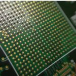
BGA packages typically contain many solder balls arranged in a dense array. During double-sided assembly, unnecessary exposure to multiple reflow cycles should be avoided when possible, particularly for components with strict thermal requirements.
Placing critical BGA or IC components on the side where they can be exposed to only one major reflow cycle may help improve process stability.
At the same time, the decision should consider:
- Package size and weight
- Solder-ball or lead pitch
- Reflow temperature requirements
- Board thickness
- PCB warpage
- Component thermal sensitivity
- Solder paste volume
- Inspection requirements
- DFM considerations
For fine-pitch components, assembly accuracy is especially important. If a component can be placed on the first side without creating mechanical or thermal conflicts, this may provide better process control in some production scenarios.
The Impact of PCB Warpage and Deformation
One of the major challenges in double-sided PCB Manufacturing is board deformation.
During the first Reflow Soldering cycle, the PCB is exposed to elevated temperatures. Differences in material properties, copper distribution, layer structure, and thermal expansion can cause slight warpage or dimensional changes.
These changes may not always be visible to the naked eye, but they can affect the accuracy of subsequent solder paste printing and component placement.
This is particularly important for:
- Fine-pitch IC packages
- BGA packages
- Small passive components
- High-density SMT areas
- Components with tight placement tolerances
For rigid-flex structures, the challenge can be even greater because rigid and flexible sections have different mechanical characteristics.
Proper support and fixturing can therefore play an important role during second-side assembly. The manufacturing team should ensure that the PCB is adequately supported during solder paste printing and component placement to minimize movement and deformation.
Solder Paste Printing Accuracy
Solder paste printing is another critical factor in SMT Assembly.
The first printing operation is performed on an unassembled surface, while the second printing operation takes place after the PCB has already experienced one complete assembly and reflow cycle.
Even small dimensional changes or board deformation can influence stencil alignment during the second printing process.
In addition, controlling the correct solder paste volume becomes more challenging when pad dimensions are small or when the PCB contains fine-pitch components.
To improve printing consistency, manufacturers should carefully control:
- Stencil design
- Aperture dimensions
- Stencil thickness
- Squeegee pressure
- Printing speed
- PCB support
- Alignment accuracy
- Solder paste condition
- Environmental conditions
For high-density PCB Design, these manufacturing considerations should be incorporated into the design-for-manufacturing process before production begins.
Optimizing the Double-Sided Assembly Sequence
There is no single assembly sequence that is suitable for every rigid-flex or double-sided PCB.
The best process should minimize the overall impact of thermal cycling, gravity, mechanical stress, board deformation, and printing variation.
A typical optimization strategy includes:
1. Identify Critical Components
Classify BGA packages, fine-pitch ICs, large connectors, heavy components, and thermally sensitive devices before determining the assembly sequence.
2. Evaluate Component Weight
Heavy components should be evaluated carefully to determine whether they are suitable for placement on the underside during the second reflow cycle.
3. Consider Thermal Requirements
Components with strict temperature limitations should be positioned and processed according to their allowable reflow profiles.
4. Analyze Board Support
Rigid-flex PCBs may require dedicated carriers, fixtures, or support structures to maintain flatness during printing and placement.
5. Verify DFM Compatibility
The proposed assembly sequence should be reviewed through DFM analysis to identify potential conflicts between component placement and manufacturing equipment.
6. Control the Second-Side Printing Process
The second printing operation should account for any dimensional changes or warpage caused by the first reflow cycle.
DFM Is Essential for Double-Sided PCB Assembly
PCB Design and manufacturing engineering cannot be treated as completely separate processes when designing a double-sided rigid-flex board.
Design-for-Manufacturing (DFM) analysis can identify potential problems before production, including insufficient component spacing, difficult-to-access pads, unsuitable component orientations, inadequate support areas, and conflicts with assembly equipment.
For rigid-flex applications, designers should also consider the transition between rigid and flexible regions. Components should generally be positioned with sufficient consideration of mechanical stress, bending requirements, and assembly support.
The design should also provide enough information for the manufacturer to determine the appropriate fixtures, carriers, stencil design, and assembly sequence.
Quality Control After Double-Sided Assembly
After both sides have been assembled, comprehensive inspection is essential.
Depending on product requirements, the inspection process may include:
- Solder paste inspection (SPI)
- Automated optical inspection (AOI)
- X-ray inspection for BGA solder joints
- Visual inspection
- Electrical testing
- Functional testing
- Dimensional inspection
For BGA and other hidden solder joints, X-ray inspection can provide additional information that cannot be obtained through conventional optical inspection.
Process data from both assembly sides should also be reviewed to identify recurring defects and improve production stability.
Kingda’s Approach to Rigid-Flex PCB Assembly
At Kingda, double-sided PCB Assembly is approached as a complete process rather than simply a sequence of component placement operations.
Our engineering team can evaluate PCB Design, component distribution, assembly orientation, thermal requirements, board support, and manufacturing conditions before production.
For complex Rigid-Flex PCB applications, careful coordination between design and manufacturing is especially important. Proper DFM evaluation and process planning can help reduce assembly risks, improve soldering consistency, and support reliable production.
Conclusion
Double-sided SMT Assembly provides an effective way to increase component density and reduce the overall size of modern electronic products. However, assembling both sides of a rigid-flex board introduces additional challenges related to component weight, multiple reflow cycles, PCB deformation, solder paste printing, and placement accuracy.
Heavy components and critical BGA Components require careful consideration when determining the assembly sequence. Fine-pitch devices also require strict control of printing and placement accuracy, particularly during second-side processing.
Ultimately, successful double-sided PCB Manufacturing depends on integrating PCB Design, DFM analysis, component placement, thermal management, fixturing, and process control into one coordinated manufacturing strategy.
By optimizing the assembly sequence according to the actual board structure and component requirements, manufacturers can improve soldering quality, reduce production risks, and achieve more reliable rigid-flex PCB assemblies.