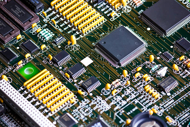
Millimeter Wave Small Cell Base Station PCB
As 5G networks continue expanding into dense environments such as urban buildings, industrial parks, transportation hubs, and smart venues, the balance between the high bandwidth potential of millimeter wave frequencies and reliable signal coverage has become a major engineering challenge.
The 5G Base Station PCB inside millimeter wave small cells plays a critical role in signal transmission, power amplification, frequency conversion, and high-speed processing. Designed specifically for high-frequency communication systems, this type of PCB requires advanced materials, precise manufacturing processes, excellent electrical performance, and strong thermal management capabilities.
A properly engineered Millimeter Wave PCB is becoming a key hardware foundation for achieving more precise and efficient 5G network coverage while preparing communication infrastructure for future high-speed wireless technologies.
Core Performance Requirements for Millimeter Wave Applications
Ultra-Low Transmission Loss
Millimeter wave signals, typically operating above 24GHz, experience significantly higher transmission loss compared with lower-frequency signals. Therefore, PCB materials must provide excellent dielectric characteristics and low signal attenuation.
Specialized materials with low dielectric constant (Dk), low dissipation factor (Df), modified PTFE materials, ceramic-filled composites, and other high-frequency substrates are commonly used to reduce transmission loss.
At frequencies such as 28GHz, advanced High Frequency PCB designs require careful control of dielectric properties, copper roughness, trace geometry, and stack-up structure to maintain signal integrity during transmission.
Low-loss materials help ensure that signals maintain sufficient strength after multiple stages of amplification and frequency conversion, supporting stable short-range indoor and outdoor coverage.
For advanced RF material selection and high-frequency PCB solutions, see High Frequency PCB Manufacturing.
Stable High-Frequency Characteristics
Millimeter wave signals are highly sensitive to physical parameter variations. Changes in temperature, humidity, and material characteristics can influence dielectric performance and affect signal stability.
A reliable RF PCB requires substrate materials with controlled thermal expansion characteristics and stable electrical properties across different operating environments.
The PCB material system should maintain consistent dielectric performance during temperature fluctuations, ensuring that communication equipment can operate reliably in outdoor installations, equipment rooms, and industrial environments.
Stable high-frequency characteristics help prevent communication interruptions caused by material property variations and ensure consistent signal transmission quality.
Efficient Thermal Management

Millimeter wave small cell base stations contain power amplifiers, mixers, RF modules, and processing components that generate significant heat during operation.
Because high-frequency circuits are sensitive to temperature changes, thermal design becomes an essential part of PCB engineering. Optimized copper distribution, large-area grounding structures, thermal vias, and dedicated heat-transfer paths help move heat away from high-power components.
A well-designed thermal structure allows heat to transfer efficiently toward external heat dissipation systems such as metal housings and cooling fins.
For compact communication equipment, thermal performance directly affects component reliability, operating stability, and long-term service life.
Strong Electromagnetic Interference Protection
The internal space of millimeter wave base stations is highly compact, with multiple RF channels, digital control circuits, and power modules operating closely together.
Without proper PCB design, electromagnetic interference and signal coupling may negatively affect communication performance.
A multilayer PCB structure separates RF signal layers, digital control layers, and power layers while incorporating grounding structures and shielding techniques around sensitive circuits.
These approaches help reduce unwanted coupling, maintain clean signal waveforms, and improve receiver sensitivity in complex electromagnetic environments.
For advanced multilayer structures designed for high-speed communication systems, see Multilayer PCB Manufacturing.
Advanced Manufacturing Technologies for High-Frequency Challenges
High-Precision Circuit Pattern Formation
Millimeter wave signals have extremely short wavelengths, meaning even small PCB geometry variations can influence signal reflection, impedance consistency, and transmission performance.
Advanced imaging technologies enable precise circuit formation with controlled trace width, spacing, and surface quality.
For high-frequency applications, maintaining accurate characteristic impedance is essential. Factors such as copper thickness, etching accuracy, line edge roughness, and dielectric thickness must be carefully controlled.
High-precision circuit manufacturing reduces impedance discontinuities and helps maintain efficient RF signal transmission.
For impedance-sensitive applications, engineers often combine simulation, stack-up optimization, and manufacturing verification. More details are available in PCB Impedance Control Design.
Microvia Manufacturing Technology
To achieve high-density multilayer interconnections while minimizing the impact of vias on high-frequency signals, millimeter wave PCBs often use microvia structures.
Laser-drilled microvias provide compact vertical connections between selected layers, allowing designers to improve routing density and reduce unnecessary signal transitions.
High-quality microvia manufacturing requires precise laser parameters, reliable copper plating, accurate positioning, and consistent hole-wall quality.
Properly manufactured microvias reduce signal reflection and insertion loss while improving electrical reliability between PCB layers.
Optimized Surface Finishing Process
RF interfaces and component pads require excellent conductivity, corrosion resistance, and solder reliability.
Surface finishes such as ENIG provide stable electrical connections while protecting exposed copper surfaces from oxidation.
For millimeter wave applications, surface treatment quality can influence connector performance, contact resistance, and impedance consistency at RF interfaces.
A properly selected surface finish helps minimize discontinuities at connection points and supports reliable high-frequency signal transmission.
Application Value Across Multiple Scenarios
Urban Building Coverage
In office buildings, shopping centers, and other dense indoor environments, traditional macro base stations often struggle to provide effective millimeter wave penetration through walls and obstacles.
Millimeter wave small cell base stations provide localized coverage through distributed deployment in corridors, ceilings, and indoor communication areas.
The low-loss characteristics of a Low Loss PCB help maintain stable signal transmission within coverage zones while supporting high-speed access for large numbers of connected devices.
PCB electromagnetic compatibility is also important in these environments because elevators, HVAC systems, lighting equipment, and other electronic devices may introduce interference.
Reliable PCB design ensures smoother experiences for applications such as cloud collaboration, augmented reality navigation, and high-definition video communication.
Industrial Manufacturing Parks
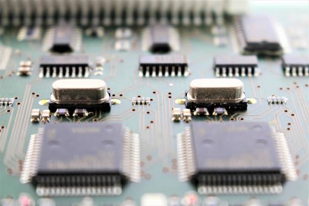
Industrial Internet applications require high bandwidth, low latency, and reliable wireless communication. Millimeter wave small cells support machine vision, industrial data transmission, automation control, and real-time equipment monitoring.
In manufacturing environments, PCBs must maintain stable high-frequency performance despite strong electromagnetic noise generated by motors, industrial controllers, and machinery.
A properly engineered 5G Base Station PCB helps maintain reliable data transmission for industrial robots, automated production lines, and intelligent manufacturing systems.
Thermal reliability is also essential because industrial environments may expose communication equipment to elevated operating temperatures for extended periods.
Transportation Hubs
Airports, railway stations, and other high-density public areas require communication systems capable of handling sudden increases in connected users.
Millimeter wave small cell base stations provide flexible deployment options in crowded environments by supporting installation on ceilings, columns, and other compact locations.
Efficient PCB thermal management helps power amplifiers and RF components maintain stable operation during periods of heavy network demand.
Through dense deployment, these systems can improve coverage capacity and reduce network congestion in high-traffic locations.
Smart Venue Applications
Sports stadiums, concert halls, and exhibition centers require extremely high bandwidth during major events due to applications such as live video streaming, augmented reality interaction, and large-scale wireless access.
Millimeter wave PCB technology enables high-speed signal transmission and supports advanced communication infrastructure for thousands of simultaneous users.
Stable electrical performance helps maintain reliable wireless connections while reducing communication errors during peak demand periods.
Future smart venues will increasingly depend on compact high-frequency communication equipment to provide immersive digital experiences.
Future Development of Millimeter Wave PCB Technology
The advancement of millimeter wave small cell PCB technology directly influences the future expansion of 5G networks and next-generation wireless communication systems.
As substrate materials, manufacturing precision, thermal solutions, and high-frequency design technologies continue improving, future Millimeter Wave PCB solutions will move toward lower transmission loss, higher integration density, improved reliability, and greater frequency capability.
These developments will provide stronger hardware support for emerging technologies such as 6G ultra-wideband communication, integrated satellite-terrestrial networks, smart cities, and advanced industrial connectivity.
Through continuous innovation in materials, design methods, and manufacturing processes, millimeter wave PCBs will remain a fundamental technology driving the evolution of high-performance wireless communication infrastructure.