4-Layer PCB Manufacturing Process: Complete Production Steps
A 4-Layer PCB Manufacturing Process combines advanced fabrication technologies and strict quality control procedures to create reliable circuit boards with higher wiring density and improved signal performance.
Compared with single-layer and double-layer PCBs, four-layer boards provide additional routing space, better electromagnetic interference control, and more stable signal transmission. They are widely used in industrial electronics, communication equipment, automotive systems, medical devices, and consumer electronics.
The production of a four-layer PCB involves multiple precision processes, including material preparation, inner layer fabrication, lamination, drilling, copper plating, outer layer pattern formation, surface finishing, and final inspection.
1. Preparation Process Before Manufacturing
The first step of the PCB Manufacturing process is selecting suitable raw materials according to product requirements.
The most important material is the copper-clad laminate (CCL). Manufacturers select different substrate materials based on electrical performance, thermal resistance, mechanical strength, and application environment.
Common materials include FR-4, high-Tg laminates, and high-frequency materials.
Before production begins, all materials must undergo strict incoming inspection to verify:
- Dielectric properties
- Copper thickness
- Thermal stability
- Mechanical strength
- Material consistency
Proper material selection provides the foundation for stable performance throughout the entire PCB Fabrication Process.
2. Inner Layer Manufacturing Process
The inner layer fabrication process is one of the most important stages in four-layer PCB production. The quality of inner circuits directly affects the reliability of the entire board.
Inner Layer Surface Preparation
Before circuit imaging, the inner layer copper surface must be cleaned and treated.
The preparation process usually includes:
- Degreasing
- Micro-etching
- Surface cleaning
Degreasing removes oil and contaminants from the copper surface, while micro-etching creates a slightly rough surface to improve photoresist adhesion.
This step ensures better circuit definition during the imaging process.
Inner Layer Circuit Formation
After surface preparation, photoresist is applied to the inner layer panel.
The main steps include:
Photoresist Coating
A layer of photosensitive material is evenly coated onto the copper surface and dried to form a protective film.
Exposure
The digital circuit design data is transferred to the PCB using Laser Direct Imaging (LDI) equipment.
The laser selectively exposes the photoresist, causing the exposed areas to harden while the unexposed areas remain soluble.
Developing
The panel is placed into a developing solution to remove the unexposed photoresist.
The remaining hardened photoresist forms the circuit protection pattern.
Copper Etching
The panel enters the etching process, where exposed copper areas are chemically removed.
The protected copper remains and becomes the designed inner layer circuit pattern.
Photoresist Stripping
After etching, the remaining photoresist is removed, revealing the completed inner circuit.
Inner Layer Inspection
After circuit formation, the inner layers undergo strict inspection.
Inspection methods include:
- Automatic Optical Inspection (AOI)
- Circuit width measurement
- Short circuit detection
- Open circuit inspection
AOI systems scan the entire circuit pattern to identify defects and ensure inner layer quality before lamination.
3. Lamination Process
Lamination is the key process that combines the inner layers, prepreg materials, and outer copper foils into a complete four-layer PCB structure.
Layer Stacking Preparation
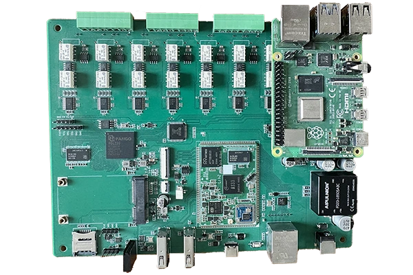
During stacking, manufacturers arrange:
- Inner circuit layers
- Prepreg materials
- Outer copper foils
according to the designed layer sequence.
Prepreg is a semi-cured fiberglass material impregnated with epoxy resin. Under heat and pressure, the resin melts and cures, bonding all layers together.
High stacking accuracy is essential to prevent layer misalignment and ensure reliable electrical connections.
Lamination Operation
The stacked PCB materials are placed into a lamination press.
The equipment applies controlled:
- Temperature
- Pressure
- Processing time
During lamination:
- The resin in the prepreg melts and flows.
- The resin fills gaps between layers.
- The materials bond together permanently.
- The cured resin forms an insulating layer.
Proper lamination control prevents defects such as:
- Delamination
- Air bubbles
- Layer shifting
- Insufficient bonding strength
For complex boards requiring complete manufacturing solutions, professional PCB Manufacturing capabilities ensure stable quality throughout production.
4. Outer Layer Processing
After lamination, the PCB enters the outer layer manufacturing stage.
This stage mainly includes drilling, hole metallization, outer circuit formation, solder mask application, and surface marking.
Drilling Process
CNC drilling machines create different types of holes according to design requirements.
These include:
- Through holes
- Component mounting holes
- Via holes
Drilling accuracy is critical because incorrect hole positioning may affect electrical connections between PCB layers.
After drilling, the board undergoes cleaning to remove debris and resin residues inside the holes.
Hole Metallization Process
Hole metallization creates electrical connections between different PCB layers.
The process includes:
Desmearing
Removing resin residues and drilling contamination from hole walls.
Electroless Copper Plating
A thin copper layer is deposited on the hole walls, making the previously non-conductive holes electrically conductive.
Electroplating
Additional copper is deposited to increase hole wall thickness and improve reliability.
This process is essential for achieving stable multilayer connections in Multilayer PCB production.
Outer Layer Circuit Formation
The outer layer circuit manufacturing process is similar to inner layer fabrication.
The main steps include:
- Photoresist coating
- LDI exposure
- Developing
- Copper etching
- Photoresist removal
Unlike inner layers, outer layer circuits must connect directly with plated through holes to complete electrical connections.
5. Solder Mask and Silkscreen Printing
Solder Mask Application
The solder mask protects PCB circuits from:
- Oxidation
- Corrosion
- Accidental short circuits
The process includes:
- Solder mask coating
- Exposure
- Developing
- Curing
Common solder mask colors include green, blue, black, and white.
Silkscreen Printing
After solder mask processing, component information is printed onto the PCB surface.
Silkscreen markings typically include:
- Component reference numbers
- Product codes
- Manufacturing information
Clear and durable markings help during component placement and maintenance.
6. Final Processing and Inspection
The final stage ensures that every four-layer PCB meets quality requirements before delivery.
Surface Finishing
Surface treatment improves solderability and protects exposed copper areas.
Common surface finishes include:
- HASL
- ENIG
- Immersion tin
- OSP
Different finishes are selected according to application requirements.
For customers requiring complete production from prototype to manufacturing, Prototype PCB Assembly solutions help validate designs before mass production.
PCB Profile Processing
According to customer specifications, CNC routing or punching equipment is used to cut the PCB into the required shape.
The process must ensure:
- Accurate dimensions
- Smooth edges
- No burrs or damage
Final Quality Testing
Before shipment, four-layer PCBs undergo comprehensive testing, including:
Electrical Testing
- Continuity testing
- Insulation resistance testing
- Open and short circuit detection
Visual Inspection
Checking:
- Solder mask quality
- Silkscreen clarity
- Surface defects
- Copper damage
Dimensional Inspection
Verifying:
- Board thickness
- Hole position
- Overall dimensions
Only products that pass all inspections can proceed to packaging and delivery.
7. Four-Layer PCB Applications
Four-layer PCBs are widely used because they provide better electrical performance and higher integration capability.
Typical applications include:
Consumer Electronics
Used in smartphones, tablets, computers, and smart devices requiring compact and reliable circuit structures.
Automotive Electronics
Applied in vehicle control systems, battery management systems, and intelligent driving modules.
Industrial Equipment
Used in automation systems, controllers, and industrial communication equipment.
Medical Devices
Provides stable signal transmission for monitoring equipment and diagnostic systems.
For electronic products requiring different assembly methods after PCB fabrication, manufacturers can provide SMT PCB Assembly and Through Hole PCB Assembly services to complete the entire production chain.
Conclusion
The 4-Layer PCB Manufacturing Process is a highly precise and systematic production procedure involving multiple critical stages, including inner layer fabrication, lamination, drilling, plating, circuit formation, surface treatment, and inspection.
Every manufacturing step requires strict process control to ensure electrical performance, mechanical reliability, and long-term stability.
With the continuous development of electronic products toward higher density, smaller size, and improved performance, four-layer PCBs will continue to play an important role in modern electronic manufacturing. Professional PCB fabrication technologies and advanced assembly capabilities provide the foundation for producing reliable and high-performance electronic solutions.