Effect of Material Hardness on PCB Manufacturing Process
During PCB Manufacturing, material hardness is an important factor that is often overlooked but plays a critical role in product quality and performance. From substrate materials and copper foils to various auxiliary materials, different hardness characteristics directly influence multiple manufacturing stages, including initial processing, circuit formation, lamination, and final assembly.
For advanced products such as high-layer-count mixed-material PCBs, high-frequency circuit boards, and HDI PCB products, precise control of material hardness is essential for achieving accurate processing, stable structures, and reliable electrical performance.
Material hardness must be carefully evaluated during PCB design and production because it affects machining efficiency, dimensional accuracy, layer alignment, and long-term durability. A proper balance between material hardness and manufacturing parameters helps ensure consistent PCB quality.
Substrate Hardness and Compatibility with Initial Processing
The substrate is the foundation of a PCB structure, and its hardness directly affects early manufacturing processes such as cutting, drilling, and surface preparation.
A substrate with suitable hardness can maintain clean edges during cutting, reduce burr formation and cracking, and provide a stable surface for subsequent circuit pattern formation. This improves processing efficiency while creating a reliable foundation for multilayer PCB assembly.
If the substrate is excessively hard, cutting tools may experience increased wear, reducing production efficiency. Excessive cutting stress may also create microscopic cracks inside the material, weakening the overall mechanical strength of the PCB.
On the other hand, if the substrate is too soft, deformation may occur during machining, making it difficult to maintain dimensional accuracy. This can negatively affect layer registration during multilayer PCB lamination.
For complex multilayer structures, consistent substrate hardness is especially important. Stable material properties ensure that each layer maintains accurate dimensions during processing and provides reliable bonding performance during lamination.
Copper Foil Hardness and Circuit Formation Performance
Copper foil is the primary conductive material in PCB structures, and its hardness characteristics significantly influence circuit formation processes such as etching and lamination.
The hardness of copper foil must be properly matched with the etching process to achieve precise circuit patterns with smooth edges and accurate line geometry.
Copper foil with suitable hardness allows etching solutions to remove unwanted copper evenly, creating clear and well-defined circuit traces. This is especially important for HDI PCB products featuring fine lines, high-density routing, and advanced interconnection structures.
If copper foil is too hard, uneven etching may occur, resulting in rough circuit edges or irregular line profiles. These defects can affect electrical performance and reduce manufacturing reliability.
If copper foil is too soft, it may become deformed or wrinkled during lamination due to uneven pressure distribution, affecting circuit integrity and layer bonding quality.
For High Speed PCB applications, copper foil hardness consistency also influences signal transmission stability. Uniform copper characteristics help maintain controlled impedance performance and reduce signal loss caused by irregular conductor shapes.
Auxiliary Material Hardness and Manufacturing Process Integration
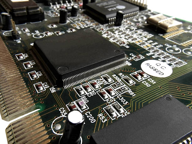
In addition to substrates and copper foils, various auxiliary materials used in PCB production, including bonding materials and solder masks, also have important hardness requirements.
The hardness of bonding materials must be compatible with both substrate and copper foil properties. Proper hardness matching ensures strong adhesion during lamination, improves interlayer bonding strength, and prevents delamination issues.
This is particularly important for high-layer-count PCB structures where multiple material interfaces must maintain long-term mechanical stability.
Solder mask hardness directly affects PCB surface protection performance. A solder mask with appropriate hardness can resist scratches, mechanical impact, and environmental stress during assembly and operation.
During the printing process, suitable solder mask hardness also helps maintain clear patterns and prevents coating damage caused by handling or friction.
However, excessive solder mask hardness may cause cracking under bending or vibration conditions, while insufficient hardness may lead to contamination, surface damage, and reduced insulation performance.
Material Hardness Control in Advanced PCB Manufacturing
Effective control of material hardness requires strict material selection, process monitoring, and manufacturing optimization.
Professional PCB manufacturers evaluate the hardness characteristics of substrates, copper foils, bonding materials, and protective coatings according to different product requirements. Material inspection ensures that all components meet production standards before entering the manufacturing process.
During production, manufacturing parameters such as cutting speed, drilling conditions, etching time, lamination pressure, and curing temperature must be adjusted according to material hardness characteristics.
This precise coordination between material properties and manufacturing processes improves production stability and reduces potential defects.
Advanced PCB production requires comprehensive quality management systems and optimized manufacturing capabilities. Through professional PCB Manufacturing Services, customers can achieve reliable solutions for complex circuit board applications requiring high precision and durability.
Influence of Material Hardness on PCB Reliability and Performance
Material hardness has a direct impact on the final performance and reliability of PCB products.
Proper hardness control improves mechanical strength, dimensional stability, and resistance to environmental stress. It helps prevent problems such as layer separation, circuit deformation, and surface damage during manufacturing and operation.
For precision applications, early validation through PCB Prototype Services allows engineers to evaluate material performance, optimize manufacturing parameters, and reduce development risks before mass production.
In high-frequency and high-density electronic systems, material hardness also contributes to electrical stability. Proper material selection supports better signal integrity, reliable impedance control, and consistent circuit performance.
Unbalanced material hardness may result in manufacturing challenges, including poor machining quality, inaccurate layer alignment, copper defects, and reduced product lifespan.
Therefore, understanding and controlling material hardness is an essential part of producing high-performance PCBs.
Advanced Material Management for High-Performance PCB Production
As electronic products continue to become smaller, faster, and more complex, PCB manufacturers must place greater emphasis on material characteristics.
The combination of advanced materials, precise processing technology, and strict quality control enables manufacturers to produce reliable circuit boards for telecommunications, automotive electronics, industrial control systems, medical devices, and other demanding applications.
Modern PCB solutions require not only advanced manufacturing equipment but also deep understanding of material behavior throughout every production stage.
Through professional Multilayer PCB Manufacturing capabilities, manufacturers can optimize material selection, layer structures, and processing techniques to meet complex application requirements.
Conclusion
Material hardness is a key factor influencing PCB manufacturing quality, process stability, and final product reliability. From substrate machining and copper foil processing to solder mask protection, every material characteristic affects the overall performance of a circuit board.
By carefully controlling PCB Material Hardness, manufacturers can improve dimensional accuracy, enhance electrical performance, and ensure long-term reliability.
With advanced manufacturing technology and strict quality management, GOPCBA provides professional PCB solutions designed to meet the requirements of high-performance electronic applications, delivering stable and reliable circuit boards for customers worldwide.