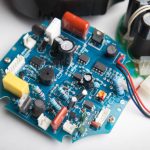
18-Layer PCB Complete Technical Guide for Engineers
13 January · In today’s rapidly evolving electronics industry, multilayer PCBs are the backbone of high-performance electronic systems. Among them, 18-layer PCBs are especially critical for applications demanding exceptional signal integrity, compact form factors, and high-density interconnects. From telecommunications infrastructure to data centers, aerospace systems, and industrial controls, these boards enable engineers to maintain reliable performance in complex circuits.
This article delivers a complete technical breakdown of 18-layer PCBs, covering design essentials, manufacturing processes, cost drivers, and real-world applications. Whether you are a PCB design engineer, hardware developer, or procurement specialist, understanding these aspects is key to optimizing your next-generation projects.

1. What is an 18-Layer PCB?
An 18-layer PCB is a multilayer printed circuit board composed of 18 alternating conductive and insulating layers. Typically, these include signal layers, power planes, and ground planes, laminated with high precision to create a high-density board capable of supporting complex electronic systems.
- High layer count: Enables separation of signals, power, and ground for dense routing.
- Excellent signal integrity: Proper ground and plane placement reduces noise and crosstalk.
- Ideal for high-speed systems: Used in 5G base stations, servers, aerospace electronics, and more.
Typical applications include telecom infrastructure, industrial automation, server motherboards, and avionics – often irreplaceable in mission-critical environments.
👉 Professional PCB design & layout services to optimize your 18-layer stackup.
2. 18-Layer PCB Stackup Design
Stackup design determines the electrical performance and mechanical stability of an 18-layer board. A typical high-performance stackup includes:

- Signal layers: 8–10 layers for high-speed routing
- Power planes: 4–5 layers for stable power distribution
- Ground planes: 3–4 layers for EMI shielding and return paths
Key design considerations:
- Impedance control: Critical for high-speed signals to prevent reflections.
- Material selection: Choose FR-4, high-Tg, or Rogers materials based on frequency and thermal requirements.
- Stackup symmetry: Prevents warpage and maintains consistent electrical behavior.
3. Key Technical Parameters
When designing an 18-layer PCB, pay close attention to these parameters:
- Minimum trace width/spacing: Advanced processes achieve 3–4 mil lines for high-density routing.
- Via types: Through-hole, blind, buried, and microvias for efficient interlayer connections.
- Surface finish: ENIG, HASL, OSP, or immersion silver for reliable solderability.
- Thermal management: Multiple copper planes help dissipate heat from high-power components.
4. 18-Layer PCB Manufacturing Process
Manufacturing 18-layer PCBs is a complex, highly controlled process:
- Lamination: Individual cores and prepregs are stacked and pressed under heat and pressure.
- Drilling & plating: Precision drilling and copper plating form interlayer connections.
- Etching & patterning: Unwanted copper is removed to define circuit traces.
- Inspection & testing: Automated optical inspection (AOI), X-ray, and impedance testing ensure quality.
Manufacturers like GoPCB provide high-precision, high-reliability 18-layer PCB production, ensuring each board meets stringent engineering requirements. Explore PCB manufacturing services for more details.
5. Performance Considerations
Engineers must account for the following when designing and using 18-layer PCBs:
- Signal integrity: Minimize crosstalk and reflections through proper stackup and routing.
- EMI/EMC: Ground planes and impedance control reduce electromagnetic interference.
- High-frequency performance: Material choice and via design affect GHz-range signal transmission.
- Mechanical & thermal reliability: Symmetric stackup and balanced copper distribution prevent warpage and thermal stress.
6. Applications of 18-Layer PCBs
18-layer PCBs are employed in industries that demand high-performance, complex circuitry:
- Telecom & 5G networks: High-speed routing and low-loss requirements.
- Data centers & servers: Dense interconnects for CPUs, GPUs, and memory modules.
- Aerospace & defense: Reliability under extreme conditions.
- Automotive & industrial controls: ADAS systems and factory automation equipment.
For tailored solutions, GoPCB turnkey assembly provides end-to-end support from prototype to volume production.
7. Cost Factors & Pricing
Several factors influence the cost of 18-layer PCBs:
- Layer count & complexity: More layers and finer features increase manufacturing difficulty and cost.
- Material choice: High-Tg or Rogers materials are more expensive than standard FR-4.
- Order quantity: Prototype units have higher per-unit costs than large-volume production.
Typical price ranges (2026 market reference):
- Prototype (5–10 pcs, 18-layer, FR-4, 1.6mm thickness): $450 – $700/pc
- Small batch (50 pcs): $300 – $500/pc
- High volume (500+ pcs): $150 – $300/pc
Lead times generally range from 15 to 25 days, depending on complexity and manufacturer capacity. For small-batch needs, check our low-volume assembly services.
8. How to Choose an 18-Layer PCB Manufacturer
Selecting an experienced manufacturer is crucial for project success. Key capabilities to look for include:
- HDI (high-density interconnect) manufacturing capability
- Rapid prototyping and on-time delivery
- Advanced testing (impedance, AOI, X-ray)
- Material expertise (FR-4, high-Tg, Rogers)
At GoPCB, we offer customized 18-layer PCB production, ensuring high reliability and performance from prototype to mass production. Our engineering team optimizes stackup and material selection for high-speed signal and thermal management – a trusted partner for high-performance PCB projects. Discover our SMT assembly services to streamline your project.
9. 18-Layer PCB FAQ
Q1: What is the typical thickness of an 18-layer PCB?
Usually between 1.6mm and 3.2mm, depending on material and copper weight.
Q2: Can I order small quantities of 18-layer PCBs?
Yes, manufacturers like GoPCB support low-volume production, though per-unit costs are higher.
Q3: What is the typical lead time for 18-layer PCBs?
Prototypes: 15–20 days; volume production: 20–35 days, depending on complexity.
Q4: How can I ensure signal integrity on an 18-layer board?
Proper impedance-controlled stackup, well-planned ground/power planes, and high-quality materials are essential.
10. Conclusion
18-layer PCBs are a critical enabler for high-density routing, impedance control, and signal integrity in advanced electronic systems. They play a vital role in telecommunications, aerospace, automotive, and industrial automation. Choosing a professional manufacturer like GoPCB ensures high-quality fabrication, rigorous testing, and cost-effective solutions from prototype to high-volume production. In your next complex PCB project, the right 18-layer partner can make all the difference.
Contact GoPCB today for your 18-layer board needs: www.gopcba.com. Explore our mixed-technology assembly and flex PCB assembly services for broader capabilities.