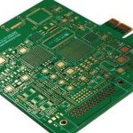
Optical Imaging PCB Solutions for Camera, LiDAR & Fiber Optic Modules
December 3, 2025 · Posted by GoPCB
As optical imaging equipment – smartphone cameras, automotive LiDAR, and fiber optic communication modules – pushes toward higher speed, miniaturization, and system integration, the PCB (printed circuit board) that underpins core performance is undergoing a dramatic transformation. From high-speed signal integrity and precision optoelectronic interconnects to thermal dissipation for laser emitters, the PCB has become the foundation that determines performance, stability, and service life. This article offers an engineering‑grade analysis of PCB solutions across various optical imaging applications, helping OEMs, hardware engineers, and procurement professionals select the optimal manufacturing approach.

1. The Critical Role of PCBs in Optical Imaging Systems
1.1 PCB as the Core Foundation
In optical imaging systems, the PCB performs multiple mission‑critical functions:
- Supporting high‑speed data processing from CMOS/CCD sensors
- Providing stable power delivery to laser emitters, photodiodes, and lens actuators
- Ensuring signal integrity and electromagnetic compatibility (EMC)
- Enabling effective thermal management
- Enabling compact form factors (e.g., stacked camera modules in smartphones)
As optical systems become smaller and data rates soar, high‑performance PCBs have become an irreplaceable enabler.
1.2 Rapid Growth Across Industries
Optical imaging PCBs are widely deployed in:

- Consumer electronics: smartphone cameras, AR/VR vision modules
- Automotive: ADAS cameras, LiDAR
- Industrial vision: inspection cameras, high‑speed scanners
- Telecom: fiber optic transceivers, optical modules
Demand for high‑precision, low‑loss, and high‑speed PCBs continues to rise across these segments.
2. Core Requirements for High‑Performance Optical Imaging PCBs
2.1 Signal Integrity for High‑Speed Optoelectronic Sensors
- Controlled impedance routing
- Low‑crosstalk layout
- Robust power/ground distribution
- Optimized differential pair routing
2.2 Superior Thermal Dissipation
Primary heat sources: image processors, VCSEL lasers, high‑speed optical chips, laser drivers.
- Metal‑core PCBs (MCPCB)
- Ceramic PCBs
- Dense thermal via arrays
2.3 Miniaturization & High‑Density Interconnect (HDI)
Optical modules are increasingly compact. HDI delivers:
- Microvias and buried vias
- Ultra‑fine line/space geometries
2.4 Low‑Loss Materials
Commonly used materials:
- Rogers 4350B
- Isola Astra MT
- Taconic series
Essential for high‑speed/high‑frequency domains such as fiber optic modules and LiDAR signal processing.
3. Camera Module PCB Design Essentials
3.1 PCB Layout for CMOS/CCD Sensors
- Minimize signal path lengths
- Use continuous ground planes
- Reduce temperature‑induced drift
3.2 EMI/EMC Control Strategies
- Shielding cans
- Ground via stitching
- Differential pair routing
3.3 Flexible PCBs (FPC) for Auto‑Focus & Zoom Systems
FPCs are widely used for:
- Lens motor drivers
- Sensor interconnects
- Multi‑layer camera module folding structures
4. PCB Solutions for LiDAR Systems
4.1 High‑Power Laser Driver PCB Requirements
- 1–3 oz thick copper
- Wide current‑carrying traces
- Excellent thermal dissipation
4.2 LiDAR Signal Processing HDI Multilayer Boards
LiDAR typically demands:
- 8–20 layer HDI
- Low‑loss materials
- BGA compatibility
4.3 Automotive‑Grade Reliability
- High‑temperature tolerance
- Vibration resistance
- Humidity and corrosion protection
5. Fiber Optic Module PCB Technology
5.1 PCBs for Common Optical Transceivers (SFP, QSFP, GPON)
- Ultra‑high bandwidth
- Strict impedance control
- High‑speed SerDes‑compatible design
5.2 Integration of Lasers & Photodiodes
- Precision pad alignment
- Ultra‑low noise power supplies
- RF‑grade routing
5.3 Low‑Crosstalk Material Selection
Megtron 6 and Rogers series provide excellent stability for high‑speed optical communication.
6. Optical Imaging PCB Material Recommendation Table
| Application | Recommended Material | Key Characteristics |
|---|---|---|
| Camera Module | FR4 / PI FPC | Low cost, flexible |
| LiDAR | Rogers 4350B / Isola 370HR | High‑frequency stability, high reliability |
| Fiber Optic Module | Rogers 3003 / Megtron 6 | Ultra‑low loss, excellent high‑speed performance |
7. GoPCB – Optical Imaging PCB Capabilities
GoPCB specializes in high‑precision optical imaging PCBs, including:
- High‑density camera module PCBs
- Low‑loss LiDAR PCBs
- High‑speed fiber optic communication PCBs
- Flex and rigid‑flex boards
Typical price ranges (USD):
- Camera PCB: $0.15 – $2.8/pcs
- LiDAR PCB: $3 – $25/pcs
- Fiber Optic Module PCB: $1.5 – $12/pcs
GoPCB supports rapid prototyping and stable volume production, with IPC‑Class 3 manufacturing capability.
Explore our prototype PCB assembly and low‑volume PCB assembly services for optical imaging projects.
8. Quality Management for Optical System PCBs
8.1 IPC Class 2 vs Class 3
Optical communication and automotive LiDAR typically require the more stringent Class 3.
8.2 Comprehensive Inspection Flow
- AOI (Automated Optical Inspection)
- X‑Ray
- Impedance testing
- Functional testing
8.3 Environmental Reliability Testing
Including high‑temperature, vibration, humidity, and thermal shock.
For high‑reliability needs, our high‑volume PCB assembly ensures consistent quality.
9. Common Challenges in Optical Imaging PCB Manufacturing
9.1 High‑Speed Signal Purity
Solutions: stable Dk/Df materials, precise differential pair matching.
9.2 Soldering of Thermal‑Sensitive Components
3. Optoelectronic Component Placement Accuracy
Especially critical for lasers, VCSELs, TOF sensors, and high‑speed connectors.
10. Optical Imaging PCB Supplier Selection Guide
10.1 Key Evaluation Criteria
- Experience with high‑frequency materials
- Microvia reliability
- High‑speed impedance control capability
- Proven automotive or optical communication case studies
10.2 Engineer’s Procurement Checklist
- Request complete stack‑up details
- Confirm material Dk/Df parameters
- Review microvia reliability reports
- Inspect copper roughness and solder mask thickness
10.3 Cost‑Performance Trade‑off
While premium materials cost more, they significantly improve image quality and device longevity.
GoPCB offers turnkey PCB assembly and SMT PCB assembly to streamline your production.
11. Conclusion
PCBs play a decisive role across all categories of optical imaging devices – from smartphone cameras to LiDAR and fiber optic modules. Only through correct material selection, precise layout, and a qualified manufacturing partner can system‑level high‑speed performance and long‑term reliability be achieved. GoPCB offers the full spectrum of manufacturing capabilities required for these demanding applications, making it an ideal partner for optical imaging PCBs.
12. FAQ
1. What is the best material for fiber optic module PCBs?
Rogers 3003 or Megtron 6 are recommended for ultra‑low loss performance.
2. Why must LiDAR use HDI PCB?
LiDAR processes massive high‑speed signals and requires high‑density interconnect structures for high‑speed data links.
3. Is FPC necessary for camera modules?
Yes, FPC is better suited for compact structures and space‑constrained auto‑focus mechanisms.
4. What are typical prices for optical imaging PCBs?
Camera: $0.15–$2.8; LiDAR: $3–$25; Fiber optic module: $1.5–$12.
5. Does GoPCB support volume production?
Yes, GoPCB supports both rapid prototyping and high‑volume stable supply.
For more on assembly options, visit our through‑hole PCB assembly and mixed‑technology PCB assembly pages.