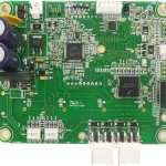
During Reflow Soldering, PCBs are exposed to rapid heating and cooling. Because a printed circuit board is a composite structure made from copper foil, resin, glass fabric, and other materials, differences in thermal expansion can generate internal stress and cause the board to bend, twist, or warp.
Severe PCB Warpage can create significant problems during SMT assembly. A warped board may not be properly supported or transported through the production line, which can affect solder paste printing, component placement, reflow soldering, inspection, and automated handling.
For high-density and high-reliability electronic products, maintaining adequate PCB Flatness is therefore an important part of PCB design and manufacturing.
The causes of PCB deformation are not limited to reflow soldering. Material selection, copper distribution, stackup symmetry, lamination, drilling, solder mask curing, hot-air solder leveling, panelization, storage, and mechanical handling can all contribute to the final board shape.
What Is PCB Warpage?
PCB Warpage refers to unwanted deformation of a PCB from its intended flat geometry.
The two common forms are:
- Bow: the board bends along a generally smooth curved surface.
- Twist: different corners of the board do not remain in the same plane.
In practical SMT production, both bow and twist can affect the ability of automated equipment to accurately handle the PCB.
The acceptable amount of deformation depends on the PCB construction, assembly process, component technology, equipment, and applicable industry or customer specifications. Therefore, a single universal warpage value should not be applied to every PCB.

Why PCB Warpage Is a Problem During Reflow Soldering
During automated SMT assembly, PCB flatness directly affects several manufacturing operations.
Solder Paste Printing
A warped PCB may not make uniform contact with the stencil. This can cause variations in solder paste deposition, especially for fine-pitch components.
Component Placement
Pick-and-place equipment requires a stable board position. Excessive deformation can affect placement accuracy or create handling problems.
Reflow Soldering
As the board passes through the reflow oven, thermal expansion and contraction can temporarily increase deformation.
For thin or large-format boards, gravity and support conditions inside the oven can further increase sagging.
Solder Joint Quality
Board deformation can alter the relative position between component terminals and PCB pads, potentially contributing to soldering defects.
Automated Handling
Severe deformation can interfere with conveyors, board clamps, support pins, inspection equipment, and other automated systems.
For these reasons, controlling PCB Deformation is important not only for the PCB itself but also for the entire PCBA manufacturing process.
Main Causes of PCB Warpage
PCB deformation generally results from a combination of thermal stress, mechanical stress, material properties, structural asymmetry, and manufacturing conditions.
1. Uneven Copper Distribution
Uneven copper distribution is one of the important contributors to PCB Warpage.
For example, one layer may contain a large copper plane while the corresponding layer contains relatively little copper. This creates an imbalance in copper content and thermal-mechanical behavior.
During heating and cooling, different areas of the PCB may expand and contract at different rates.
A more balanced copper distribution can help reduce this imbalance.
For multilayer boards, designers should consider:
- Copper area on each layer
- Plane distribution
- Signal routing density
- Power and ground planes
- Symmetry between corresponding layers
- Localized copper concentration
Copper balancing is especially important for large, thin, and multilayer PCBs.
2. Asymmetric PCB Stackup
A symmetrical stackup generally provides better mechanical balance than a highly asymmetric structure.
If the thickness, copper content, dielectric material, or resin distribution differs significantly between the two sides of the board, thermal expansion can become unbalanced.
During lamination and subsequent thermal processing, this imbalance can generate residual stress and contribute to deformation.
Therefore, PCB Design should consider stackup symmetry from the beginning of the design process.
3. Different Coefficients of Thermal Expansion
A PCB is composed of multiple materials, and each material has its own coefficient of thermal expansion (CTE).
Copper, resin, glass fabric, solder mask, and other materials do not necessarily expand and contract at the same rate.
The glass fabric reinforces the resin system and influences the dimensional stability of the laminate. The resin system also changes its mechanical behavior significantly around its glass transition temperature.
These differences create internal stress during thermal cycling.
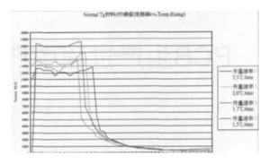
4. Glass Transition Temperature
The glass transition temperature (Tg) is the temperature range at which the resin system changes from a relatively rigid glassy state toward a softer, more rubber-like state.
When the PCB temperature approaches or exceeds its Tg, the resin’s mechanical properties change significantly, and the board becomes more susceptible to deformation under thermal and mechanical stress.
This is why High-Tg PCB materials are often considered for applications involving lead-free reflow, repeated thermal exposure, high operating temperatures, or demanding reliability requirements.
However, a higher Tg does not automatically eliminate PCB warpage. Laminate CTE, modulus, resin content, copper distribution, stackup, processing conditions, and board geometry also play important roles.
5. Board Size and Thickness
Large and thin PCBs are generally more susceptible to deformation because their structural stiffness is lower.
During reflow, the board is transported through the oven while being supported by the conveyor system. If the board is large, heavy, or insufficiently supported, its own weight can cause sagging.
Increasing board thickness can improve mechanical stiffness, but the final solution must balance flatness requirements against product size, weight, electrical performance, and mechanical constraints.
6. Vias and Interlayer Connections
Multilayer PCBs contain many interlayer connections, including through vias, blind vias, and buried vias.
Copper structures can constrain local expansion and contraction of the surrounding laminate. When these structures are distributed unevenly, they can contribute to internal stress.
Vias themselves are not inherently a cause of warpage. The overall distribution of copper, resin, holes, and stackup structure is more important.
7. V-Scoring and Panelization
V-scoring removes part of the material between individual boards in a production panel.
Although V-scoring is useful for depanelization, the remaining material has reduced mechanical stiffness compared with a continuous panel.
Poorly selected scoring depth, board geometry, or panel layout can increase deformation during processing and handling.
Depending on the PCB design, routed tabs, perforated tabs, or other panelization methods may provide a better mechanical solution.
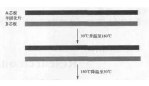
Material and Structural Effects on PCB Deformation
Material Properties
The dimensional stability of a PCB is strongly influenced by the properties of its laminate system.
Important characteristics include:
- Tg
- CTE
- Resin content
- Glass fabric structure
- Elastic modulus
- Moisture absorption
- Thermal stability
- Copper foil characteristics
Different laminate systems can therefore behave differently during lamination, reflow, and thermal cycling.
Copper Distribution
Copper does not merely provide electrical conductivity. It also contributes to the mechanical and thermal behavior of the finished board.
If the copper pattern is highly asymmetric, the two sides of the board can respond differently during heating and cooling.
For this reason, copper balancing should be considered during PCB Design, especially for multilayer and large-format boards.
Lamination Structure
During PCB Lamination, prepreg flows and cures while the board is subjected to pressure and temperature.
The final laminate structure depends on:
- Core thickness
- Prepreg selection
- Resin content
- Copper distribution
- Pressing temperature
- Pressure profile
- Heating and cooling rate
- Tooling configuration
An unbalanced lamination structure can retain residual stress that is released during later manufacturing steps.
PCB Deformation During Manufacturing
PCB Manufacturing includes multiple thermal and mechanical processes that can affect board flatness.
Copper-Clad Laminate
Copper-clad laminate is generally a relatively balanced structure, but its large dimensions and the thermal characteristics of the press equipment can still produce localized differences in curing and stress.
Uneven temperature distribution across the press area may cause different regions to cure at slightly different rates.
PCB Lamination
Lamination is one of the most important stages affecting board deformation.
During lamination, the PCB experiences high temperature and pressure. Resin flows, fills the spaces between copper patterns, and eventually cures.
If different areas of the board have substantially different resin content or copper density, the resulting stress distribution may become uneven.
Symmetrical stacking and appropriate press parameters can help reduce these effects.
Drilling and Mechanical Processing
Drilling, routing, V-scoring, profiling, and other mechanical processes introduce localized mechanical stress.
These stresses can release residual stress that was retained during earlier lamination processes.
The board may therefore appear flat after lamination but develop deformation later in the manufacturing flow.
Solder Mask Curing
Solder mask curing exposes the board to elevated temperatures.
If a thin board is supported poorly during curing, its own weight and thermal stress can contribute to deformation.
Proper rack spacing, support, orientation, and curing conditions should therefore be considered.
Hot Air Solder Leveling
Hot Air Solder Leveling (HASL) exposes the PCB to a high-temperature soldering environment followed by cooling.
The rapid thermal transition can produce temporary and residual thermal stress.
The exact process temperature and exposure time depend on the equipment, solder alloy, board construction, and process settings. They should not be treated as universal values.
Storage and Handling
PCB deformation can also occur during storage.
Improper stacking, excessive weight, insufficient support, or unsuitable storage conditions can mechanically deform thin PCBs.
Because laminate materials have a degree of viscoelastic behavior, deformation caused by long-term mechanical loading may not completely disappear after the external force is removed.
How to Reduce PCB Warpage
Several approaches can be combined to control PCB Deformation.
1. Optimize the Reflow Thermal Profile
Reflow temperature should be established according to the solder paste, components, PCB materials, and assembly requirements.
Instead of simply lowering the oven temperature, the goal should be to achieve an appropriate heating and cooling profile while meeting soldering requirements.
Excessively rapid heating or cooling can increase thermal stress, while an inappropriate profile can cause soldering defects.
Therefore, thermal-profile optimization should be based on actual process measurements.
2. Use Suitable High-Tg Materials
Using a High-Tg PCB material can improve thermal stability in applications requiring repeated high-temperature processing.
However, material selection should consider the complete laminate system, including:
- Tg
- Z-axis CTE
- X-Y dimensional stability
- Moisture behavior
- Thermal decomposition characteristics
- Mechanical strength
- Electrical performance
High Tg alone should not be regarded as a complete solution for PCB warpage.
3. Increase PCB Thickness When Possible
Increasing board thickness generally increases mechanical stiffness and can reduce sagging during reflow.
A thicker PCB may be beneficial for large boards, heavy components, or assemblies requiring strong mechanical support.
However, product requirements may limit board thickness. In such cases, panelization, support tooling, stackup optimization, and reflow fixtures may provide alternative solutions.
4. Optimize PCB Size and Panelization
Reducing the unsupported span of a PCB can reduce sagging during reflow.
Panel design should consider:
- Board dimensions
- Conveyor direction
- Board orientation
- Component weight distribution
- Tooling requirements
- Depanelization method
- Support points
The longest dimension of the board should be evaluated together with the conveyor and support structure rather than applying a universal orientation rule.
5. Use Reflow Support Fixtures
For thin, large, or mechanically sensitive boards, a reflow support fixture or carrier can significantly improve mechanical stability.
The fixture supports the PCB while it passes through the reflow oven, reducing sagging caused by gravity.
For particularly flexible or thin boards, customized tooling may provide more consistent support than the standard conveyor alone.
Fixture material and design must also account for thermal expansion, oven temperature, component clearance, board loading, and production efficiency.
6. Optimize the Depanelization Method
If V-scoring creates excessive mechanical weakness, alternative panelization methods should be considered.
Depending on the board design, routed tabs, perforations, or hybrid depanelization methods may provide better mechanical performance.
The objective is to balance manufacturing efficiency, edge quality, PCB strength, and assembly requirements.
PCB Design Strategies for Warpage Control
Controlling deformation should begin during the design stage rather than waiting until final inspection.
Maintain Stackup Symmetry
For multilayer PCBs, the dielectric and copper structure should be evaluated for symmetry around the board’s central plane whenever the design allows.
Balance Copper Content
Designers should avoid extreme copper-density differences between opposing layers.
Copper balancing may involve adjusting copper pours, planes, dummy copper, or routing distribution while maintaining electrical and manufacturing requirements.
Avoid Excessive Structural Asymmetry
Asymmetry in:
- Layer construction
- Copper thickness
- Copper pattern
- Dielectric thickness
- Resin distribution
- Large mechanical cutouts
can increase deformation risk.
Not every PCB can be perfectly symmetrical, so manufacturing compensation may be necessary for special structures.
Consider Heavy Components
Large transformers, connectors, heatsinks, batteries, and other heavy components can increase mechanical loading during reflow.
Component weight distribution should therefore be considered during PCB and assembly design.
Improving Lamination to Reduce Warpage
Proper PCB Lamination control is essential for multilayer PCB flatness.
Symmetrical Lay-Up
Where possible, core materials, prepregs, copper foils, and tooling materials should be arranged symmetrically.
Control Heating and Cooling
The heating and cooling profile should be appropriate for the laminate system.
Rapid temperature transitions can generate additional thermal stress.
Controlled cooling can help reduce residual stress in some board constructions.
Optimize Press Parameters
Press temperature, pressure, vacuum, heating rate, cooling rate, and dwell time should be established according to the material system and PCB construction.
There is no single pressing recipe suitable for every multilayer PCB.
Use Appropriate Tooling
Tooling plates, separator materials, release materials, and press configurations can influence heat transfer and mechanical constraint.
For complex or asymmetric structures, tooling design may need to be customized.
Can Asymmetric Lamination Be Used?
Although symmetrical construction is generally preferred, some products cannot avoid asymmetric structures.
In these cases, controlled asymmetric lamination may sometimes be used to compensate for predictable dimensional behavior.
The principle is to modify the thermal and mechanical conditions of the stackup so that the final board approaches the required flatness after cooling.
This should be treated as an engineering optimization rather than a universal production method.
Actual results should be verified through trial production, dimensional measurement, and process capability analysis.
PCB Leveling Before Shipment
PCB manufacturers may perform leveling before shipment when board deformation exceeds the applicable requirements.
Mechanical leveling or thermal leveling can be used depending on the PCB construction.
Thermal leveling involves controlled heating and cooling to reduce residual deformation.
However, leveling should not be used as a substitute for controlling the root causes of warpage.
If the PCB repeatedly develops deformation because of an unbalanced stackup, copper distribution, lamination process, or improper storage, simply leveling the finished board may provide only temporary improvement.
For high-reliability production, the preferred approach is to control deformation throughout the manufacturing process.
Other Manufacturing Factors Affecting PCB Flatness
Several additional factors should be considered.
Board Support During Thermal Processing
Thin boards should be adequately supported during high-temperature processes.
Poor support can allow gravity to produce permanent deformation while the resin system is in a softened state.
Storage Orientation
Boards should be stored in a way that minimizes long-term mechanical loading.
Large stacks of unsupported thin boards should be avoided.
Cooling After High-Temperature Processes
Rapid cooling can increase thermal stress.
Where appropriate, controlled cooling can help reduce the difference in thermal contraction between different materials and structures.
Moisture Control
Moisture absorbed by the laminate can influence dimensional stability and thermal behavior.
Proper material storage and preconditioning should therefore be considered, particularly before high-temperature processing.
PCB Flatness Inspection
Controlling PCB Flatness requires measurement rather than visual inspection alone.
Depending on the application, manufacturers may evaluate:
- Board bow
- Board twist
- Local deformation
- Dimensional stability
- Thickness variation
- Warpage after thermal exposure
Inspection can be performed at different manufacturing stages to identify where deformation is introduced.
For high-volume production, trend monitoring and statistical process control can help identify gradual changes in material or process behavior.
A Practical PCB Warpage Control Strategy
A systematic approach can be summarized as follows:
PCB Design → Material Selection → Stackup Optimization → Copper Balancing → Lamination Control → Mechanical Processing → Thermal Processing → Storage → Flatness Inspection
Each stage can contribute to the final board shape.
For example, a board that is already under residual stress after lamination may become more deformed during drilling, solder mask curing, HASL, or reflow.
Therefore, the most effective solution is to identify the stage where the deformation originates and address the underlying process rather than relying only on final-board correction.
Kingda’s Approach to PCB Warpage Control
At Kingda, PCB flatness is considered throughout the product development and manufacturing process.
For multilayer, thin, large-format, HDI, and other demanding PCB structures, key factors can be reviewed during engineering evaluation, including:
- Material selection
- PCB stackup
- Copper distribution
- Board thickness
- Panelization
- Lamination parameters
- Mechanical processing
- Thermal processing
- Reflow compatibility
- Storage and handling
- Final flatness inspection
For boards with asymmetric structures or particularly demanding flatness requirements, engineering trials and process adjustments can be used to identify the most suitable manufacturing approach.
The objective is not simply to correct a warped board at the end of production, but to minimize deformation from the beginning of the manufacturing process.
PCB Warpage Prevention Checklist
Before mass production, designers and manufacturers should review:
- Is the PCB stackup sufficiently balanced?
- Is copper distribution reasonably balanced?
- Are the laminate materials appropriate for the thermal process?
- Is the Tg and CTE suitable for the application?
- Is the board too large or too thin for the intended assembly equipment?
- Are heavy components distributed appropriately?
- Is the panelization method mechanically suitable?
- Are V-score or routed-tab dimensions appropriate?
- Are lamination parameters optimized?
- Are boards properly supported during thermal processing?
- Is the reflow profile validated?
- Are storage and handling conditions controlled?
- Is PCB flatness measured according to the applicable specification?
Conclusion
PCB Warpage is a complex manufacturing issue caused by the interaction of materials, thermal stress, mechanical stress, copper distribution, stackup structure, processing conditions, and handling.
Reflow Soldering can expose existing stress and temporarily increase board deformation, but the root causes often originate much earlier during material selection, PCB Design, lamination, panelization, and mechanical processing.
Using appropriate materials, balanced copper distribution, a well-designed stackup, controlled PCB Lamination, suitable panelization, proper thermal processing, and effective support fixtures can significantly reduce the risk of PCB Deformation.
For demanding applications, controlling PCB Flatness should be treated as a complete engineering process rather than a final inspection activity. By identifying deformation risks early and coordinating design with manufacturing, Kingda can help customers achieve more stable PCB production and reliable SMT assembly performance.