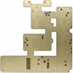
In the era of smartphones and highly integrated electronic devices, manufacturers are constantly challenged to make products smaller, thinner, lighter, and more functional. Behind this development is a critical technology: the printed circuit board.
As electronic systems continue to integrate more functions into increasingly compact spaces, conventional PCB technologies face limitations in wiring density, thermal management, signal integrity, electromagnetic compatibility, and component integration.
This has accelerated the development of advanced Multilayer PCB technologies, high-density interconnects, embedded components, advanced materials, and increasingly sophisticated manufacturing processes.
China has developed into one of the world’s major PCB manufacturing regions. The industry’s development has also gradually shifted from relatively labor-intensive production toward higher-value manufacturing supported by engineering expertise, automation, advanced materials, precision equipment, and process innovation.
Today, the ability to manufacture advanced PCBs is an important indicator of a manufacturer’s overall technical and engineering capabilities.
Scientific and Technical Challenges in Advanced PCB Development
Wherever electronic information technology exists, PCBs are an essential part of the system.
From smartphones and communication equipment to automotive electronics, industrial controls, medical devices, and computing platforms, PCBs provide the electrical interconnection between components and subsystems.
However, the rapid development of modern electronics has created new technical requirements.
Electronic products increasingly demand:
- Higher wiring density
- Smaller feature sizes
- More layers in limited board thickness
- Higher signal transmission rates
- Better thermal management
- Improved electromagnetic compatibility
- Greater mechanical reliability
- More integrated component structures
- Higher manufacturing precision
These requirements have pushed PCB Technology beyond conventional circuit fabrication.
A modern high-density board may combine multilayer construction, microvias, fine-line circuits, controlled impedance, advanced surface finishes, and specialized dielectric materials.
The challenge is no longer simply to manufacture a circuit board. Manufacturers must ensure that electrical, mechanical, thermal, and manufacturing requirements are satisfied simultaneousl
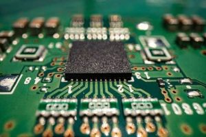
From Conventional PCB Fabrication to High-Density Integration
Traditional PCB manufacturing generally relies on subtractive circuit formation, mechanical drilling, lamination, plating, and surface treatment.
These technologies remain fundamental, but increasingly dense designs require additional process capabilities.
For example, advanced High-Density Interconnect structures can use microvias to create shorter interconnection paths and improve routing efficiency.
Depending on the product architecture, manufacturers may also use:
- Laser-drilled microvias
- Sequential lamination
- Via-in-pad structures
- Fine-line circuitry
- High-layer-count stackups
- Controlled-impedance structures
- Advanced copper plating
- Low-loss dielectric materials
- Embedded passive components
The appropriate technology depends on the electrical and mechanical requirements of the application.
Using advanced technology simply for the sake of complexity is not necessarily beneficial. A well-engineered PCB structure should achieve the required performance while maintaining manufacturability, reliability, and reasonable cost.
High-Density PCB Materials
Materials play a fundamental role in advanced PCB development.
As circuit density and operating frequency increase, standard materials may not always provide the required electrical or thermal performance.
Depending on the application, manufacturers may evaluate materials based on:
- Dielectric constant (Dk)
- Dissipation factor (Df)
- Glass transition temperature (Tg)
- Coefficient of thermal expansion (CTE)
- Thermal conductivity
- Moisture resistance
- Copper adhesion
- Dimensional stability
- Copper roughness
- Processing compatibility
For high-speed communication systems, the dielectric properties of the laminate can have a significant influence on signal propagation and loss.
For high-power applications, thermal conductivity and the complete thermal path become more important.
Therefore, PCB Materials should be selected according to the actual electrical, thermal, mechanical, environmental, and manufacturing requirements of the final product.
High-Density Interconnect Technology
High-Density Interconnect technology is an important development in modern PCB manufacturing.
Unlike conventional through-hole structures, microvias can provide shorter vertical interconnections and greater routing flexibility.
HDI structures can be particularly useful when designers need to route signals from fine-pitch packages such as BGA and other high-density components.
Depending on the design, HDI manufacturing may involve:
- Material preparation
- Inner-layer circuit fabrication
- Lamination
- Laser drilling
- Desmear and surface conditioning
- Copper metallization
- Microvia formation
- Sequential build-up
- Outer-layer circuit fabrication
- Surface finishing
- Electrical testing
Each stage requires accurate process control.
For example, microvia reliability depends on factors including via geometry, dielectric thickness, copper structure, plating quality, thermal cycling, and the overall stackup.
Consequently, high-density PCB manufacturing requires close cooperation between design engineering and fabrication engineering.
The Importance of Fine-Line Manufacturing
As electronic devices become smaller, the available routing area decreases while the number of electrical connections continues to increase.
This creates demand for finer line widths and smaller spacing.
Fine-line manufacturing requires precise control of:
- Photoresist imaging
- Exposure
- Development
- Etching
- Copper thickness
- Registration
- Surface condition
- Inspection
Manufacturing capability should always be evaluated in relation to the actual material system, copper thickness, board structure, line geometry, and production volume.
A manufacturer capable of producing a very fine line in one construction may not necessarily achieve the same capability across every PCB structure.
Therefore, process capability should be verified against the actual design rather than represented by a single headline number.
Embedded Components and Integrated PCB Structures
Another direction in advanced PCB development is the integration of passive components into the PCB structure.
Depending on the technology and design, resistors, capacitors, inductive structures, or other functional elements may be incorporated into the board.
The potential benefits include:
- Reduced component count on the surface
- More efficient use of board area
- Shorter electrical connections
- Improved packaging density
- Greater design flexibility
However, embedded structures also introduce manufacturing and inspection challenges.
Engineers must consider material compatibility, process tolerances, repairability, testing, thermal behavior, and long-term reliability before adopting embedded-component technology.
Thermal Management in High-Density PCB Design
Higher integration means more functions are concentrated in a smaller physical area.
As a result, thermal management becomes increasingly important.
High-density PCB development should consider the complete heat path from the component to the surrounding environment.
Possible thermal solutions include:
- Larger copper areas
- Thermal vias
- Copper planes
- Heat spreaders
- Thermal interface materials
- Metal-core PCB structures
- Improved airflow
- Heat sinks
- Optimized component placement
However, adding thermal vias or copper alone does not automatically solve a thermal problem.
The effectiveness of a thermal design depends on the complete thermal path, material properties, interface resistance, airflow, component power dissipation, and system-level cooling architecture.
Signal Integrity and Electromagnetic Compatibility
As signal speeds increase, PCB performance becomes increasingly dependent on transmission-line behavior and return-current paths.
Advanced PCB Technology therefore needs to consider signal integrity and electromagnetic compatibility during the early design stage.
Important design factors include:
- Controlled impedance
- Reference-plane continuity
- Return-current paths
- Differential-pair routing
- Via transitions
- Crosstalk
- Power integrity
- Grounding strategy
- Component placement
- High-frequency material selection
For high-speed interfaces, simply reducing trace length is not enough. Designers must also maintain appropriate impedance and a continuous reference environment.
Similarly, electromagnetic interference cannot be solved by grounding alone. It requires coordinated control of noise sources, coupling paths, return currents, power distribution, shielding, and PCB layout.
From Research to Industrial Manufacturing
The development of advanced PCB Innovation depends on more than laboratory research.
Successful commercialization requires technologies to be translated into stable, repeatable manufacturing processes.
This transition involves:
- Process development
- Equipment selection
- Material qualification
- Pilot production
- Process capability evaluation
- Quality control
- Reliability testing
- Production optimization
- Engineering training
A technology may demonstrate excellent performance in a laboratory environment but still require significant engineering work before it can be applied consistently to mass production.
Therefore, collaboration between research institutions, material suppliers, equipment manufacturers, PCB manufacturers, and electronic product companies can accelerate the transfer of new technologies into commercial applications.
The Role of Automation in Modern PCB Manufacturing
Automation is becoming an increasingly important part of advanced PCB Manufacturing.
Automated and semi-automated systems can improve production consistency, reduce manual handling, increase data traceability, and support real-time process monitoring.
Typical applications include:
- Automated material handling
- CNC drilling
- Laser drilling
- Automated optical inspection
- Electrical testing
- Dimensional measurement
- Automated plating control
- Production data collection
- Process traceability
However, automation should be integrated with engineering and quality systems.
The objective is not simply to increase machine utilization, but to create a more stable and measurable manufacturing process.
Quality and Reliability as Competitive Advantages
For high-density circuit boards, quality control must extend throughout the manufacturing process.
Important inspection and testing methods may include:
AOI Inspection
Automated optical inspection can identify visible circuit-pattern defects such as opens, shorts, missing copper, and registration problems.
Electrical Testing
Electrical testing verifies connectivity and helps detect unintended opens and shorts.
X-Ray Inspection
X-ray inspection can be used to examine internal structures that are not visible from the board surface, particularly when advanced packages or internal structures require additional verification.
Microsection Analysis
Microsection analysis can evaluate internal copper thickness, plated-hole quality, layer registration, resin distribution, and other construction characteristics.
Reliability Testing
Depending on the application, testing may include thermal stress, solderability, insulation resistance, impedance verification, thermal cycling, and other reliability evaluations.
The specific inspection plan should be based on product requirements, industry standards, customer specifications, and risk assessme.
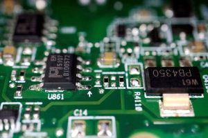
Building China’s Advanced PCB Industry
China’s PCB Industry has developed significantly alongside the growth of consumer electronics, telecommunications, automotive electronics, industrial equipment, and computing.
The next stage of development is increasingly focused on moving toward higher-value products and stronger technical capabilities.
Several areas are particularly important:
Advanced manufacturing technology
Manufacturers need to continuously improve high-density fabrication, precision registration, drilling, plating, lamination, and surface treatment.
Material capabilities
The development and application of high-performance dielectric materials will become increasingly important for high-speed, high-frequency, and high-temperature applications.
Automation and digital manufacturing
Production data, automated inspection, process monitoring, and traceability can improve manufacturing consistency.
Engineering talent
Experienced engineers remain essential for process development, DFM analysis, troubleshooting, and product qualification.
Quality systems
Stable processes and comprehensive quality control are fundamental to long-term customer relationships.
Kingda’s Role in Advanced PCB Manufacturing
For advanced PCB projects, the relationship between design and manufacturing is particularly important.
Kingda can support customers through engineering review, material selection, stackup evaluation, DFM analysis, multilayer fabrication, drilling, plating, surface finishing, electrical testing, and final inspection.
For complex Multilayer PCB designs, early communication with the manufacturer can help identify potential manufacturing risks related to:
- Layer registration
- Fine-line structures
- Via design
- Board thickness
- Copper distribution
- Lamination
- Impedance control
- Surface finish
- Thermal requirements
- Assembly compatibility
By combining engineering expertise with controlled PCB Manufacturing processes, Kingda aims to provide reliable PCB solutions for increasingly demanding electronic applications.
Future Development of Advanced PCB Technology
The evolution of electronic products will continue to create new requirements for PCB manufacturers.
Future development is likely to focus on:
- Higher wiring density
- Smaller interconnect structures
- Higher-speed signal transmission
- Lower-loss materials
- Better thermal management
- Greater component integration
- More intelligent manufacturing
- Improved reliability
- More sustainable production
The development of advanced PCBs is therefore not based on a single breakthrough technology.
Instead, it depends on the coordinated development of materials, equipment, design methodology, manufacturing processes, inspection technology, and engineering expertise.
Conclusion
The evolution of China’s PCB Industry demonstrates how PCB manufacturing is moving from conventional production toward increasingly sophisticated, technology-driven manufacturing.
The growing demand for thinner, smaller, faster, and more functional electronic products is driving the development of Multilayer PCB, High-Density PCB, High-Density Interconnect, advanced materials, embedded structures, and intelligent manufacturing.
For PCB manufacturers, long-term competitiveness depends on more than production capacity. Technology, quality, engineering expertise, automation, material knowledge, and manufacturing consistency are becoming equally important.
With continuous investment in PCB Innovation and process improvement, manufacturers such as Kingda can help support the next generation of compact, high-performance, and reliable electronic products.