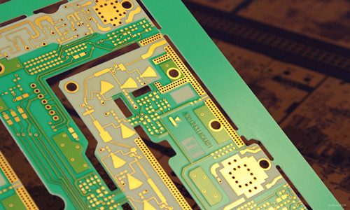
High-speed interconnects are fundamental to modern electronic systems. As communication equipment continues to operate at higher frequencies and data rates, PCB manufacturers and designers face increasing challenges in maintaining signal integrity, thermal stability, manufacturing consistency, and long-term reliability.
These requirements have accelerated the development of High-Frequency PCB technologies for telecommunications, RF systems, wireless infrastructure, automotive electronics, aerospace applications, and other high-performance electronic products.
For modern RF and high-speed systems, PCB performance is no longer determined by circuit design alone. The electrical and thermal characteristics of the substrate, copper foil, dielectric system, layer structure, and manufacturing process can all influence the final performance of the product.
In particular, the development of advanced PCB Materials is becoming increasingly important as system bandwidth, operating frequency, and power density continue to increase.
Key Requirements for High-Frequency PCB Applications
From an RF system perspective, modern communication equipment is facing several major technical challenges.
Compared with previous-generation systems, today’s RF equipment may require:
- Wider operating bandwidth
- Higher transmission frequencies
- Higher RF output power
- Lower insertion loss
- More stable electrical performance
- Improved thermal dissipation
- Greater manufacturing consistency
- Better environmental performance
These requirements place higher demands on the complete PCB structure.
For example, increasing frequency can make dielectric loss and conductor loss more significant. At the same time, higher power levels can increase heat generation, which may affect material properties and long-term reliability.
As a result, three areas have become particularly important in advanced RF PCB development:
Electrical consistency, thermal management, and environmental performance.
1. Why Material Selection Matters for High-Frequency PCBs
The substrate is one of the most important components of a high-frequency circuit.
Conventional FR-4 materials remain suitable for many general-purpose PCB applications. However, when a circuit operates at higher frequencies or requires very low transmission loss, designers may need to consider specialized High-Frequency Materials.
The electrical performance of a PCB substrate is influenced by several parameters, including:
- Dielectric constant (Dk)
- Dissipation factor (Df)
- Dielectric loss
- Frequency stability
- Copper surface roughness
- Thermal expansion
- Moisture absorption
- Thermal conductivity
- Dimensional stability
Dk and Df are especially important in RF applications.
A stable dielectric constant helps maintain predictable impedance and signal propagation characteristics, while a low dissipation factor can reduce dielectric loss during high-frequency transmission.
However, there is no single material that is ideal for every RF application. Material selection should be based on operating frequency, transmission distance, impedance requirements, power level, thermal conditions, layer structure, and manufacturing requirements.
Therefore, engineers should evaluate the complete system rather than selecting a material based on one specification alone.
2. High-Frequency PCB and Signal Integrity
As operating frequency increases, PCB traces can no longer be treated simply as conductive connections.
They behave as transmission lines whose electrical characteristics are influenced by trace geometry, dielectric properties, reference-plane configuration, copper roughness, and surrounding structures.
This makes signal integrity a critical consideration in High-Frequency PCB design.
Important factors include:
- Controlled impedance
- Trace width and thickness
- Dielectric thickness
- Copper roughness
- Reference-plane continuity
- Via structures
- Connector transitions
- Differential-pair geometry
- Crosstalk
- Return-current paths
Even relatively small variations in PCB manufacturing can affect high-frequency performance.
For example, changes in dielectric thickness or trace geometry may shift characteristic impedance. Similarly, excessive copper roughness can increase conductor loss, particularly at higher frequencies because of the skin effect.
For demanding RF Applications, the PCB design and material selection must therefore be considered together.
3. Thermal Management in High-Power RF Applications
Increasing RF power creates another major challenge: heat.
As RF amplifiers, power devices, converters, and other components operate at higher power levels, more heat must be transferred away from the component and PCB.
Poor thermal management can result in:
- Higher operating temperatures
- Electrical performance drift
- Material degradation
- Reduced component lifetime
- Increased thermal stress
- Lower overall system reliability
For this reason, PCB Thermal Management is an important part of high-power RF design.
Possible approaches include:
- High-thermal-conductivity PCB materials
- Large copper areas
- Thermal vias
- Copper-filled vias
- Heat spreaders
- Metal structures
- Heat sinks
- Thermal interface materials
- Optimized component placement
- Improved airflow
The thermal path should be evaluated as a complete system rather than focusing on an individual PCB feature.
A typical thermal path can be represented as:
RF Component → Package → PCB Copper → Thermal Structure → Heat Sink or Chassis → Ambient Environment
The effectiveness of this thermal path depends on the component’s power dissipation, copper distribution, dielectric properties, thermal interfaces, enclosure structure, and operating environment.
4. High-Thermal-Conductivity PCB Materials
The development of high-power RF equipment has increased demand for PCB substrates with improved thermal characteristics.
Traditional PCB materials may provide adequate electrical performance for many applications, but higher power density can require additional thermal capability.
High-thermal-conductivity materials can help transfer heat away from high-power components and reduce localized temperature increases.
When evaluating advanced PCB Materials, engineers should consider both electrical and thermal characteristics.
Important parameters may include:
- Thermal conductivity
- Dk
- Df
- CTE
- Glass-transition temperature
- Decomposition temperature
- Moisture resistance
- Dimensional stability
- Copper adhesion
- Lamination compatibility
A material with excellent thermal conductivity is not necessarily the best choice if its RF characteristics, manufacturability, or reliability are unsuitable for the application.
Therefore, electrical performance and thermal performance should be optimized together.
5. RF PCB Materials and Insertion Loss
Insertion loss is another important consideration in high-frequency communication systems.
As the signal travels through the PCB, energy can be lost through dielectric and conductor mechanisms.
The major contributors may include:
- Dielectric loss
- Conductor loss
- Copper roughness
- Surface effects
- Impedance discontinuities
- Connector transitions
- Via structures
At higher frequencies, copper surface roughness can become particularly important.
Because high-frequency currents tend to concentrate near the conductor surface, the effective electrical path can be influenced by the roughness of the copper foil.
Using appropriately selected low-roughness copper can help reduce conductor loss in demanding RF transmission structures.
Therefore, RF PCB material selection should include not only laminate characteristics but also copper foil properties.
6. Controlling Passive Intermodulation in RF PCBs
Passive intermodulation, commonly known as PIM, can become a significant issue in RF communication systems.
PIM occurs when passive components or structures generate unwanted intermodulation products under strong RF signals.
Potential contributors include:
- Connectors
- Copper interfaces
- Surface contamination
- Mechanical joints
- Antenna structures
- Poor contact surfaces
- Material or structural nonlinearities
For high-power communication equipment, reducing PIM requires careful attention to materials, surface finishes, mechanical connections, grounding, and manufacturing consistency.
PCB design and manufacturing processes can therefore contribute to overall RF performance.
Proper material selection, controlled copper characteristics, accurate fabrication, and reliable assembly can help reduce potential sources of unwanted RF interference.
7. Thermal Reliability and Long-Term PCB Performance
Temperature changes can create mechanical stress within a PCB because different materials expand at different rates.
The coefficient of thermal expansion (CTE) is therefore an important consideration for high-reliability applications.
Repeated heating and cooling cycles can cause mechanical stress between:
- Copper
- Dielectric materials
- Plated through-holes
- Microvias
- Components
- Solder joints
Over time, excessive thermal stress may contribute to cracking, delamination, via reliability problems, or other failures.
For this reason, PCB Reliability should be evaluated under realistic operating conditions.
Material selection should consider not only initial electrical performance but also how those properties change during the expected service life of the product.
8. Environmental Considerations for PCB Materials
Environmental requirements are also becoming increasingly important in PCB manufacturing.
Many electronic products are moving toward halogen-free material systems where required by customer specifications, regulations, or environmental objectives.
The selection of environmentally responsible PCB Materials should consider:
- Halogen content
- Manufacturing emissions
- Material recyclability
- Chemical compliance
- Waste management
- Product lifecycle requirements
However, environmental performance should not be evaluated separately from electrical and thermal performance.
For advanced RF applications, the material must still provide appropriate dielectric characteristics, thermal stability, mechanical reliability, and manufacturing compatibility.
The goal is to achieve a practical balance between technical performance, environmental requirements, cost, and production feasibility.
9. The Importance of Manufacturing Consistency
For high-frequency applications, material selection alone cannot guarantee PCB performance.
Manufacturing consistency is equally important.
Critical manufacturing parameters may include:
- Line width
- Line spacing
- Copper thickness
- Dielectric thickness
- Layer registration
- Surface roughness
- Plating thickness
- Lamination quality
- Via dimensions
- Impedance control
Small dimensional variations can influence electrical characteristics, particularly in high-frequency transmission lines.
Therefore, PCB Manufacturing processes should be tightly controlled when producing RF and high-speed boards.
Designers should also communicate manufacturing requirements early in the development process.
A DFM review can help identify potential problems involving material selection, stackup configuration, impedance control, copper distribution, via structures, and fabrication tolerances before production begins.
10. Designing High-Frequency PCBs for Performance and Reliability
A successful High-Frequency PCB design requires more than selecting a low-loss laminate.
The entire board architecture should be considered.
Designers should evaluate:
- Signal paths
- Return-current paths
- Reference planes
- Impedance requirements
- Power distribution
- Thermal paths
- RF isolation
- Grounding
- Component placement
- Manufacturing tolerances
For example, an RF trace should maintain a consistent transmission-line environment from the source to the destination.
Sudden changes in trace width, dielectric thickness, reference-plane structure, or via geometry can introduce discontinuities.
Similarly, high-power RF components should be positioned so that their thermal paths are short and efficient.
This demonstrates why electrical, thermal, mechanical, and manufacturing considerations must be integrated during PCB development.
11. Kingda’s Approach to High-Frequency PCB Manufacturing
For demanding RF and communication applications, close cooperation between the PCB designer and manufacturer can improve the overall development process.
Kingda can support customers with PCB fabrication for applications requiring advanced multilayer structures, controlled impedance, high-density routing, high-frequency materials, and demanding manufacturing tolerances.
Engineering evaluation can cover areas such as:
- Material selection
- Stackup design
- Controlled impedance
- Trace geometry
- Copper thickness
- Surface finish
- Via structures
- Lamination
- Layer registration
- Thermal considerations
- Electrical testing
For high-frequency applications, early engineering communication is especially important.
By reviewing the design before fabrication, potential DFM issues can be identified earlier, helping improve manufacturability, consistency, reliability, and production efficiency.
12. Future Development of High-Frequency PCB Technology
As communication systems continue to evolve, the demand for advanced High-Frequency PCB solutions is expected to increase.
Future development will likely focus on:
- Lower-loss dielectric materials
- Higher-frequency operation
- Improved copper technology
- Better thermal conductivity
- Higher wiring density
- More precise impedance control
- Advanced HDI structures
- RF and digital integration
- Improved manufacturing automation
- Higher long-term reliability
At the same time, PCB manufacturers must balance electrical performance with cost, manufacturing capability, environmental requirements, and supply-chain considerations.
The most effective PCB solution is not necessarily the most technologically advanced material or structure.
Instead, the optimal solution is the one that provides the required electrical, thermal, mechanical, manufacturing, and reliability performance at an appropriate cost.
Conclusion
The continued development of high-speed and high-frequency electronic systems is creating increasingly demanding requirements for PCB technology.
For RF and communication applications, High-Frequency PCB performance depends on the interaction between material properties, circuit design, copper characteristics, thermal management, manufacturing precision, and reliability.
Selecting suitable PCB Materials is therefore only one part of the solution.
Designers and manufacturers must also consider signal integrity, insertion loss, thermal performance, PIM, impedance control, and manufacturing consistency throughout the development process.
By combining appropriate materials with controlled manufacturing processes and engineering expertise, Kingda can support customers developing reliable PCB solutions for demanding RF Applications, high-power communication equipment, and next-generation electronic systems.