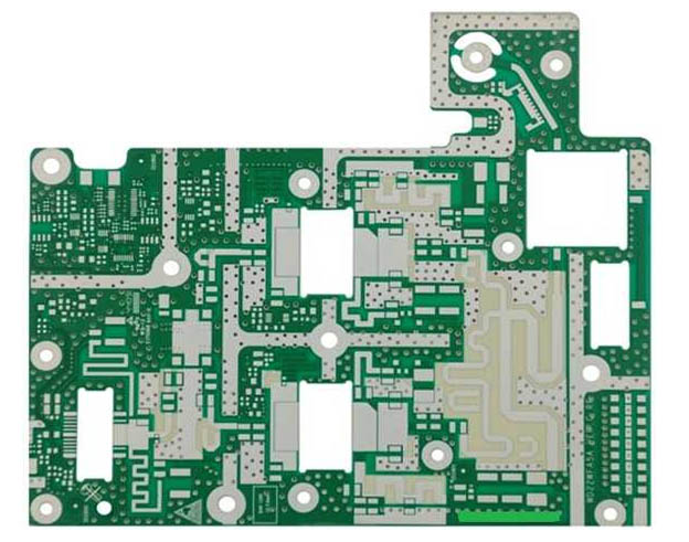
RO4350B PCB is widely used for high-frequency and high-speed electronic applications that require stable electrical performance, low dielectric loss, and reliable manufacturing characteristics.
As operating frequencies continue to increase, conventional FR-4 materials may not provide sufficient electrical performance for certain RF and microwave applications. Designers therefore need to select a PCB Material based on dielectric properties, thermal stability, dimensional stability, manufacturability, and overall cost.
RO4350B is a glass-reinforced, ceramic-filled hydrocarbon thermoset laminate designed to provide high-frequency electrical performance while maintaining processing characteristics that are closer to conventional epoxy/glass PCB materials.
This combination makes RO4350B suitable for RF amplifiers, antennas, filters, impedance-controlled transmission lines, power amplifiers, and other microwave circuits.
Electrical Performance of RO4350B
One of the primary advantages of RO4350B PCB is its stable high-frequency electrical performance.
At high frequencies, signal loss becomes increasingly important. The dielectric properties of the substrate directly affect propagation characteristics, impedance, insertion loss, and overall RF performance.
Important electrical parameters include:
- Dielectric constant (Dk)
- Dissipation factor (Df)
- Frequency stability
- Thermal stability
- Dimensional stability
- Copper surface characteristics
- Impedance consistency
A stable dielectric constant helps designers establish predictable transmission-line dimensions and impedance. Low dielectric loss can also help reduce signal attenuation, especially in longer RF transmission paths.
For this reason, High-Frequency PCB designs should evaluate the complete electrical performance of the laminate rather than focusing on a single material specification.
Why RO4350B Is Used for RF PCB Applications
As operating frequency increases, material selection becomes increasingly important.
Conventional FR-4 is widely used because of its low cost, availability, and excellent general-purpose manufacturing characteristics. However, its dielectric loss and frequency-dependent electrical properties may not be ideal for demanding RF and microwave circuits.
RO4350B was developed to provide RF performance while retaining relatively conventional PCB manufacturing characteristics.
This makes the material attractive for applications such as:
- RF and microwave circuits
- Antenna systems
- Wireless communication equipment
- Power amplifiers
- RF filters
- Coupling networks
- Impedance-controlled transmission lines
- High-frequency industrial electronics
- Radar and communication systems
The appropriate material should always be selected according to the operating frequency, signal bandwidth, power level, thermal environment, and reliability requirements of the application.
Low-Loss Characteristics
For an RF PCB, signal loss can generally be divided into several components, including dielectric loss and conductor loss.
Dielectric loss is strongly associated with the dissipation factor of the substrate. Conductor loss is influenced by copper resistivity, conductor geometry, frequency, and copper surface roughness.
Therefore, selecting a low-loss PCB Material is only one part of reducing overall channel loss.
PCB designers should also consider:
- Transmission-line length
- Copper thickness
- Copper roughness
- Trace geometry
- Impedance matching
- Via transitions
- Connector transitions
- Dielectric thickness
A material with good high-frequency characteristics provides a strong foundation, but proper PCB Manufacturing and circuit design are equally important.
Thermal and Dimensional Stability
Thermal stability is another important characteristic of RO4350B PCB applications.
High-frequency circuits may operate at elevated temperatures, particularly in power amplifiers, communication equipment, and other high-power RF systems.
The laminate’s thermal characteristics influence:
- Dimensional stability
- Via reliability
- Lamination performance
- Thermal cycling reliability
- PCB warpage
- Registration accuracy
RO4350B has a high glass transition temperature, which helps maintain structural stability over a broad processing and operating temperature range.
For multilayer RF boards, this is particularly important because repeated thermal exposure can cause dimensional changes that affect registration and plated through-hole reliability.
Coefficient of Thermal Expansion (CTE)
The coefficient of thermal expansion, or CTE, describes how much a material changes dimensionally as temperature changes.
For a multilayer High-Frequency PCB, CTE compatibility between the dielectric material and copper is important.
Large differences in thermal expansion can place additional mechanical stress on plated through-holes and other interconnections during thermal cycling.
A material with suitable X-, Y-, and Z-axis expansion characteristics can therefore improve long-term PCB reliability.
The Z-axis CTE is especially important because excessive expansion in this direction can increase stress on plated through-hole walls during heating and cooling cycles.
For high-reliability applications, CTE should be evaluated together with copper thickness, via structure, aspect ratio, layer count, and expected thermal cycling conditions.
RO4350B PCB Drilling Performance
PCB drilling is an important part of PCB Manufacturing, especially for multilayer RF boards with a large number of plated through-holes and vias.
One advantage of RO4350B is that it can generally be processed using drilling and fabrication techniques similar to those used for conventional epoxy/glass PCB materials.
However, the exact drilling parameters should be established according to:
- Board thickness
- Copper thickness
- Hole diameter
- Drill diameter
- Stack height
- Drill tool geometry
- Spindle speed
- Feed rate
- Material construction
- Required hole-wall quality
Drill quality should be evaluated based on actual hole-wall performance rather than simply measuring drill-tool wear.
Important inspection items include:
- Hole-wall roughness
- Hole diameter
- Hole position
- Resin smear
- Burr formation
- Copper integrity
- Plated through-hole quality
Proper drilling conditions help reduce defects and improve the reliability of subsequent desmear, plating, and via formation processes.
Drill Tool Life and Hole Quality
During production, drill-tool life should not be determined solely by the number of hits.
The actual condition of the drilled holes is more meaningful when evaluating tool performance.
As a drill wears, it may produce:
- Increased hole-wall roughness
- Larger burrs
- Dimensional variation
- Poor hole positioning
- Increased heat generation
- Resin damage
Therefore, manufacturers should establish tool-life criteria based on both tool condition and actual hole quality.
For PCB Drilling, appropriate process monitoring is particularly important for high-density multilayer boards where small variations in hole quality can affect plating reliability.
Processing Compatibility
Unlike many PTFE-based microwave laminates, RO4350B is designed to be processed using manufacturing techniques that are closer to those used for standard epoxy/glass PCB materials.
This can reduce the need for specialized processing and simplify manufacturing.
Typical processes can include:
- CNC drilling
- Mechanical routing
- Imaging
- Etching
- Lamination
- Desmear
- Copper plating
- Solder mask application
- Surface finishing
- Electrical testing
However, this does not mean that all process parameters should simply be copied from standard FR-4 production.
The selected material construction, copper foil, board thickness, stack-up, and finished tolerances should be considered when establishing the manufacturing process.
Preparation for RO4350B PCB Fabrication
Proper preparation is important before manufacturing a RO4350B PCB.
Input and Output Materials
During mechanical drilling, rigid and sufficiently flat entry and backup materials should be used to support the board and minimize burr formation.
Suitable entry materials may include aluminum or rigid composite panels, depending on the production process.
The backup material should provide adequate support without causing excessive mechanical stress or damaging the PCB surface.
Board Stack-Up
The total drilling stack height should be selected according to the drill diameter, board thickness, aspect ratio, and required hole quality.
Excessive stack height can increase drilling resistance and heat generation and may negatively affect hole-wall quality.
For high-reliability boards, manufacturers should validate drilling conditions through process testing rather than relying only on theoretical calculations.
Surface and Copper Considerations
Copper surface characteristics can influence high-frequency electrical performance.
At higher frequencies, the skin effect causes current to concentrate closer to the conductor surface. Therefore, copper roughness can contribute to conductor loss.
For long RF transmission lines, designers may need to consider lower-profile copper to reduce high-frequency conductor loss.
However, copper roughness should be balanced against adhesion and manufacturing reliability.
A smoother copper surface may provide electrical advantages, but the complete material and fabrication system must still provide sufficient bonding strength and reliability.
Material Availability and Construction Options
Different glass-cloth constructions and dielectric thicknesses can be used to achieve different PCB stack-ups.
The choice of glass style and resin content affects:
- Dielectric thickness
- Resin distribution
- Dk characteristics
- Impedance
- Lamination behavior
- Dimensional stability
For impedance-controlled RF circuits, the dielectric construction should be selected together with the transmission-line geometry.
This is particularly important for multilayer boards where multiple dielectric constructions may be combined within the same stack-up.
Design Considerations for RO4350B PCB
When designing an RF PCB with RO4350B, engineers should consider the complete RF signal path.
Important design factors include:
Controlled Impedance
Transmission lines should be designed according to the target impedance and actual dielectric construction.
Signal Routing
RF traces should be kept as short and direct as practical, with unnecessary discontinuities minimized.
Grounding
A stable reference plane is essential for controlled RF transmission and return-current paths.
Via Design
Vias can introduce inductive and capacitive discontinuities. Their diameter, spacing, anti-pad dimensions, and connection to reference planes should therefore be carefully designed.
Connector Transitions
RF connectors should be designed together with the PCB launch structure to minimize impedance discontinuities.
Thermal Management
High-power RF circuits require adequate thermal paths to prevent excessive temperature rise and maintain stable electrical performance.
RO4350B and FR-4: When Should You Choose Each?
FR-4 remains an excellent choice for many general-purpose PCBs because it provides a good balance of cost, availability, mechanical performance, and manufacturability.
However, specialized high-frequency materials such as RO4350B may be more appropriate when electrical loss, frequency stability, or RF performance becomes a critical design requirement.
The choice should be based on actual application requirements rather than automatically selecting the most advanced material.
For example:
| Requirement | Typical Material Consideration |
|---|---|
| General digital electronics | Standard FR-4 may be sufficient |
| Moderate-speed digital circuits | Improved low-loss materials may be considered |
| RF and microwave circuits | High-frequency materials such as RO4350B may be appropriate |
| High-power RF applications | Low-loss and thermally stable materials should be evaluated |
| Precision impedance-controlled circuits | Material Dk stability and thickness tolerance are critical |
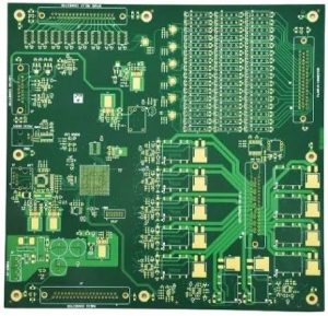
Kingda’s Role in High-Frequency PCB Manufacturing
Selecting the correct material is only the first step in producing a reliable RO4350B PCB.
Kingda can support high-frequency PCB projects by integrating material selection with PCB stack-up design and manufacturing process control.
Important manufacturing capabilities include:
- High-frequency PCB fabrication
- Multilayer PCB manufacturing
- Controlled impedance production
- Precision mechanical drilling
- Copper plating
- Fine-line fabrication
- Surface treatment
- Electrical testing
- Dimensional and registration control
- Quality inspection
For RF applications, early communication between the PCB designer and manufacturer is particularly important.
The manufacturer should understand the target frequency, impedance requirements, material construction, copper thickness, hole requirements, and expected operating environment before production begins.
Conclusion
RO4350B PCB technology provides a useful combination of high-frequency electrical performance and relatively conventional PCB manufacturing characteristics.
Its RF performance, thermal stability, dimensional stability, and compatibility with established fabrication processes make RO4350B suitable for many RF, microwave, antenna, filter, and communication applications.
However, material selection alone does not guarantee high-frequency performance. PCB Drilling, copper roughness, impedance control, stack-up design, via structures, grounding, connector transitions, thermal management, and overall PCB Manufacturing quality must all be controlled.
For demanding High-Frequency PCB projects, engineers should evaluate electrical performance, mechanical reliability, manufacturing capability, and total cost together. With proper material selection and process control, Kingda can help customers manufacture reliable RF PCB solutions that meet demanding performance and reliability requirements.