Edge Computing Gateway PCB: Design, Manufacturing and Cost Guide
What an Edge Computing Gateway PCB Does
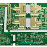
An edge computing gateway sits between field devices, industrial networks and the cloud, and its printed circuit board is the hardware foundation for data collection, protocol conversion, local calculation, artificial intelligence inference, secure communication and remote management. Unlike a simple communication module, the gateway must process information locally instead of uploading everything to the cloud, which places unusual demands on the board that carries the processor, memory and interfaces.
A typical edge computing gateway PCB integrates a high performance CPU or AI processor, DDR memory, industrial Ethernet, Wi-Fi and Bluetooth, 4G or 5G cellular modules, CAN bus, RS232 and RS485 industrial interfaces, USB and PCIe high speed links, power management, a security encryption chip and local storage. Because these subsystems run on the same board and often operate in an industrial cabinet, the PCB layout must balance high speed digital signals with noisy power stages and long industrial cables.
These boards are found in industrial automation, smart factories, intelligent transportation, smart energy, medical equipment, robots and AI vision systems. In each application the gateway PCB is expected to work continuously for years, which is why PCB design layout decisions made early have a much bigger effect on total cost than the component price alone.
Architecture and Subsystems of the Gateway Board
The heart of the gateway is the processor section. Industrial gateway boards commonly use an application processor with several cores, and newer designs add a neural processing unit for on-device AI tasks such as defect detection, predictive maintenance and video analysis. Around the processor sits the memory subsystem: DDR memory for runtime data and eMMC or managed flash for the operating system and local storage. The power architecture must generate clean, low noise rails for the core, the I/O and the radio, and the sequencing of these rails is normally defined by the processor vendor.
The communication section is what makes the board a gateway. Industrial Ethernet with isolation transformers connects to the plant network, while CAN and RS485 connect to programmable logic controllers, sensors and drives. Cellular modules provide wide area connectivity, and Wi-Fi and Bluetooth cover local wireless devices. Each interface has different impedance, common mode and surge requirements, so the schematic must treat them as separate design domains even though they share one board.
Security is increasingly built into the hardware. A secure element or trusted platform module stores keys for encrypted communication with the cloud, and the board layout should keep this section separated from user accessible interfaces. Local storage must also tolerate power loss, because a gateway in a remote cabinet cannot rely on clean shutdowns.
High Speed Design Rules That Decide Performance
Edge gateway boards are high speed designs even when their clock rates look modest. DDR buses, PCIe, USB 3.0 and gigabit Ethernet all need controlled impedance traces, matched lengths and solid reference planes. The layer stack should place signal layers adjacent to continuous ground planes, and the board manufacturer must hold the dielectric thickness and etch tolerances that the impedance calculation assumes.
Signal integrity problems in gateways usually appear as intermittent failures rather than complete stops. A marginal DDR timing issue may only fail when the temperature rises inside the cabinet, and a poorly routed Ethernet pair may only show errors under long cable conditions. Designers should therefore budget for the right number of layers instead of forcing a high speed layout into a minimum cost stack. A common configuration is eight layers for a full gateway with DDR4, PCIe and multiple gigabit interfaces.
Electromagnetic compatibility deserves the same attention as signal integrity. Gateways sit near motors, inverters and radio transmitters in industrial environments, so filtering, shielding and grounding must be designed in from the start. The enclosure and the PCB work together: ground stitching around connector areas, ferrite on external cables and careful placement of switching regulators all reduce the risk of EMC failures during certification.
Material Selection for an Industrial Environment
Standard FR-4 is adequate for many gateway boards, but the operating environment determines the right grade. Boards installed in unheated cabinets, outdoors, or near heat sources need a laminate with a higher glass transition temperature so the material keeps its dimensional stability and insulation resistance over time. For repeated high speed signals, low loss material may be specified for the outermost high speed layers, although most designs can keep the full stack in FR-4 if the layout is disciplined.
Copper weight is usually standard one ounce for signal layers, with heavier copper on power stages that carry the current of cellular transmitters or PoE inputs. The surface finish is chosen by reliability and assembly method: immersion gold gives flat pads and long shelf life for fine pitch BGAs and edge connectors, while cheaper finishes may be acceptable for boards with mostly standard packages. For industrial products that must survive humidity and vibration, the finish and the conformal coating decision should be made together with the assembly process.
Manufacturing and Assembly Challenges
Fabricating an edge gateway PCB combines several difficult features on one board: fine pitch BGAs, high layer counts, controlled impedance, mixed hole sizes and possibly blind or buried vias. The fabricator must be able to hold tight registration between layers, plate small vias reliably and test the finished boards for opens, shorts and impedance. These capabilities separate a serious industrial board supplier from a simple prototype shop, and they directly affect yield and delivery time.
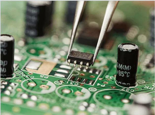
Assembly is equally demanding because the board mixes technologies. The processor and memory are placed by high accuracy SMT equipment, while power connectors, industrial terminal blocks, RJ45 jacks and shielded module sockets may need through-hole or press-fit processes. Boards with cellular modules also need careful handling of the shielded cans and antenna contacts. A SMT PCB assembly line that can place fine pitch BGAs and then complete selective soldering for the through-hole parts is essential for a reliable gateway build.

Testing the Finished Gateway Board
Because a gateway combines computing, networking and industrial I/O, functional test coverage is more valuable than a long list of generic checks. After automated optical inspection confirms the solder joints, in-circuit test verifies the power rails and the connectivity of the BGA and connector networks. The board is then powered and each subsystem is exercised: memory is stress tested, Ethernet ports exchange traffic, USB and PCIe devices are enumerated, and the industrial interfaces communicate with test equipment.
For products with cellular radios, the RF path should be verified at board level so that antenna tuning problems are found before the final enclosure is assembled. Thermal testing matters too, because a gateway running AI inference generates sustained heat; a board that works on the bench may still fail if the power stage overheats inside the enclosure. Suppliers that document the PCBA testing results give the buyer confidence that the boards shipped match the qualified sample.
Cost Drivers and How to Control Them
An edge computing gateway PCB is one of the more expensive industrial board types because it combines high layer count, controlled impedance, fine pitch assembly and extensive testing. The layer count is usually the largest fabrication cost factor, followed by the finish, the via technology and the panel utilization of the board shape. On the assembly side, the processor and memory components dominate the material cost, while BGA placement, X-ray inspection and functional test dominate the labor cost.
Cost can be controlled without cutting quality. Sharing a standard layer stack and board size across several gateway models improves panel utilization and fabrication learning. Keeping the design to proven processors and modules reduces the risk of rework, and ordering fabrication and assembly together avoids the overhead of coordinating two suppliers. Industrial buyers who consolidate their gateway volume with one industrial PCBA partner usually see lower per-board cost than buyers who split the order across multiple shops.
Working With a Full Service Partner
Edge gateway products bring design, fabrication, assembly and testing together in one program, and the smoothest path is a supplier that can review the layout for manufacturability before the boards are ordered. A DFM review at the design stage can improve the layer stack, adjust via sizes, correct pad geometry for the BGA and recommend test points, which reduces cost and improves first pass yield more than any later optimization.
gopcb manufactures and assembles edge computing gateway PCBs under one roof, from controlled impedance multilayer fabrication through fine pitch SMT placement, selective soldering and functional testing. The engineering team reviews the high speed layout, suggests stack and panel improvements, and provides documentation that follows the board through PCB manufacturing to final test. Send gopcb your gateway schematic, layout files and annual volume for a free DFM review and a quotation that reflects the real cost of a reliable industrial board.