Filter PCB Cost Guide: 2026 Pricing, Materials and Design Factors
What a Filter PCB Is and Where It Is Used
A filter PCB is a printed circuit board designed to perform electronic filtering, using inductors, capacitors, microstrip lines and stripline structures to pass wanted frequencies while suppressing noise, spurious signals and electromagnetic interference. Filter boards are not a single product family; they range from simple low pass networks on a two layer board to precision RF filters that rely entirely on the printed structure of the laminate. In 2026 these boards are found in 5G communication equipment, base station antenna systems, Wi-Fi routers, GPS modules, satellite communications, automotive millimeter wave radar, medical imaging, industrial automation and IoT terminals.
Because filter PCBs mainly carry high frequency signals, they generally need controlled impedance, high precision etching, low dielectric loss materials and a tightly controlled manufacturing process. Those requirements are the reason a filter board usually costs more than an ordinary FR-4 board of the same size, and they are also the reason buyers should evaluate a quotation by the electrical results, not by comparing it with standard PCB prices.
Reference Prices for Filter PCBs in 2026
Market prices for custom filter PCBs in 2026 vary strongly with board type. A simple two layer FR-4 filter board for prototyping typically costs between 40 and 120 US dollars including engineering and tooling; in small to medium batches the per board price falls to roughly 4 to 10 dollars, and in high volume production it can drop to about 0.8 to 3 dollars per board. These figures apply to ordinary FR-4 boards where the filtering function is implemented mainly with discrete components.
Prices rise sharply when the board must work at high frequency. An RF filter board using low loss material, tight impedance control and precise line geometry can cost 3 to 10 times more than an equivalent FR-4 board, because the laminate is more expensive and the yield is lower. Boards for automotive millimeter wave radar and satellite links, where the printed structure itself forms the filter, are quoted almost individually, and small batches frequently cost several hundred dollars per board before assembly.
The correct way to read these numbers is as a framework rather than a tariff. Every filter PCB quotation depends on the frequency of operation, the substrate, the layer count, the line width and spacing, the surface finish and the required testing, and two boards with the same outline can differ in price by an order of magnitude when one is a simple audio filter and the other is a millimeter wave band pass filter.
Why Substrate Choice Dominates the Cost
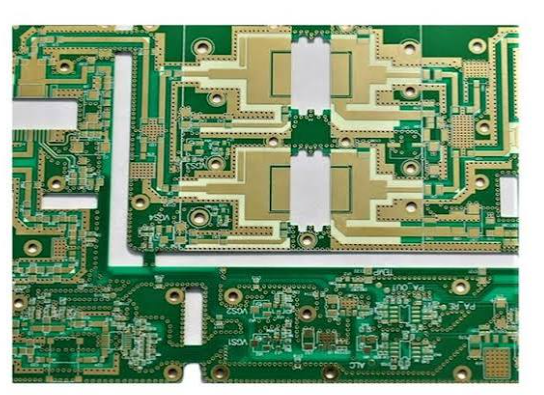
The substrate is the largest cost driver for a real filter PCB. Standard FR-4 has a dielectric constant around 4.2 to 4.6 with a loss tangent near 0.020, which is acceptable below roughly one gigahertz but increasingly lossy at higher frequencies. When the filter must handle 2.4 GHz Wi-Fi, 5G bands, or millimeter wave radar, the designer selects a high frequency laminate with a stable dielectric constant and a loss tangent an order of magnitude lower, and the material price rises accordingly.
Material consistency matters as much as the headline loss value. A filter realized with printed microstrip resonators depends on the dielectric constant and the thickness of the laminate staying within tight limits across the whole panel; if the material varies, the center frequency of the filter shifts. High frequency laminates therefore carry tighter electrical tolerances, and suppliers that can quote a specific material grade, thickness and copper weight, rather than a generic RF material, deliver boards that actually meet the specification.
Low loss laminates also require gentler processing. They are softer than FR-4, absorb moisture differently and need adapted drilling, routing and plating parameters. A fabricator that handles high frequency material regularly will have better yields than one that treats it as an occasional special job, which is a hidden cost factor that shows up in the delivered price per good board.
Design Complexity and Impedance Control
The electrical design of a filter board decides how difficult the board is to manufacture. Discrete LC filters are comparatively forgiving, while distributed filters built from microstrip or stripline resonators demand precise line widths, consistent dielectric spacing and accurate etching. When the filter operates at several gigahertz, a small variation in line width can shift the response out of specification, so the fabricator must hold tighter tolerances than standard production allows.
Impedance control adds its own cost. Controlled impedance boards require coupon testing, tighter process windows and sometimes additional layers to provide continuous reference planes. For a filter PCB the impedance of the transmission lines is part of the circuit design, not just a signal integrity nicety, so the layer stack and the material thickness must be defined together with the electrical simulation before the board is quoted.
Layer Count and Surface Finish
Many filter boards are single or double sided, but complex devices combine a filter section with active circuits, shielding and multiple supplies, which pushes the board to four, six or more layers. Every added layer pair increases lamination, drilling and plating cost, and on high frequency material the price step between layer counts is larger than on FR-4 because the material waste and process risk grow together.
Surface finish is selected for RF performance and reliability. Immersion gold gives a flat, corrosion resistant surface with consistent skin effect behavior and is the common choice for boards that carry high frequency signals and fine pitch components. Some designs use immersion silver for lower cost RF applications, while HASL is avoided where the surface must stay flat and predictable. The finish choice interacts with assembly too: a board that must be reliable in outdoor base station equipment needs a finish that survives humidity, temperature cycling and long storage.
Assembly and Testing of Filter Boards
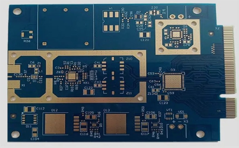
Filter PCBs are often assembled in mixed technology, with small surface mount filters, inductors and capacitors beside larger connectors and shielding cans. The assembly process must respect the frequency of the design: component placement accuracy, solder volume and ground stitching all affect the final electrical response, so the assembler should follow the layout notes from the RF engineer rather than treating the board as a standard product.
Testing is where filter boards differ most from ordinary PCBs. Beyond electrical test of the bare board, many filter boards need RF measurements such as return loss, insertion loss and rejection at specific frequencies, either on sample basis or on every board depending on the application. For automotive radar and satellite hardware, the manufacturer must keep the RF test data with the batch records so that any field issue can be traced to a specific board and process step. Full service suppliers combine this RF verification with general PCBA testing so the customer receives one complete quality record.
How to Lower Filter PCB Cost
Cost reduction for a filter PCB starts with material selection. If the operating frequency allows FR-4 or a mid range RF laminate, moving away from an exotic substrate can cut material cost dramatically, and a small change in the required dielectric tolerance can let the fabricator use a standard lot instead of a special buy. Second, the design should use the largest line widths and spacings that still meet the filter response, because fine features reduce yield and raise inspection cost on every high frequency board.
Third, panel utilization matters on expensive material. High frequency laminates are bought in expensive panels, and a board outline that wastes area can add more to the unit cost than the layer stack. Working with the manufacturer to combine several filter designs on one panel, or to adjust the outline without changing the circuit, is one of the most effective savings available. Fourth, testing depth should be matched to the application: full RF test on every board is essential for radar and satellite work, but unnecessary for a filter that only needs a functional check.
Finally, order consolidation reduces overhead. Combining fabrication with SMT PCB assembly keeps the RF material, the assembly parameters and the test records under one quality system, and it removes the coordination cost of moving expensive boards between separate suppliers.
Choosing a Manufacturer for Filter PCBs
A manufacturer chosen for filter PCB work should demonstrate three capabilities: experience with low loss and RF laminates, controlled impedance processing with documented coupons, and RF measurement capability or a trusted test partner. The quotation should state the material grade, the dielectric thickness, the impedance target and the test plan, because those details determine whether the delivered board will match the design simulation.
gopcb fabricates filter PCBs on high frequency laminates and assembles them with fine pitch SMT placement and RF aware processes. The engineering team reviews the filter layout, selects the substrate that meets the frequency and loss budget, and coordinates bare board testing with assembly so the final PCB manufacturing record includes the electrical verification the product needs. Send gopcb your filter design files and operating frequency for a free DFM review and a 2026 quotation with material, impedance and test options.