As electronic systems continue to operate at higher frequencies and faster data rates, PCB designers must pay increasing attention to high-frequency PCB design and signal integrity. At high frequencies, PCB traces are no longer simple electrical connections. Their geometry, reference planes, dielectric materials, vias, return paths, and surrounding structures all affect electrical performance.
Four major factors should be considered when designing a high-frequency PCB:
- PCB power noise
- Transmission line interference
- PCB coupling and crosstalk
- EMI interference
Proper control of these factors helps reduce signal distortion, reflection, electromagnetic radiation, crosstalk, and power integrity problems.
1. PCB Power Noise
Power noise can have a significant impact on high-frequency signals. Therefore, a low-noise power distribution network is one of the fundamental requirements of high-frequency PCB design.
Clean power and a clean ground system are equally important.
A practical power distribution network always has some impedance. Because this impedance is distributed across the PCB, transient currents can create voltage fluctuations and noise on the power network.
The basic relationship can be expressed as:
V = I × Z
where V is the noise voltage, I is the transient current, and Z is the impedance of the power distribution path.
Therefore, reducing power-distribution impedance is an important way to control power noise.
1.1 Use Dedicated Power and Ground Planes
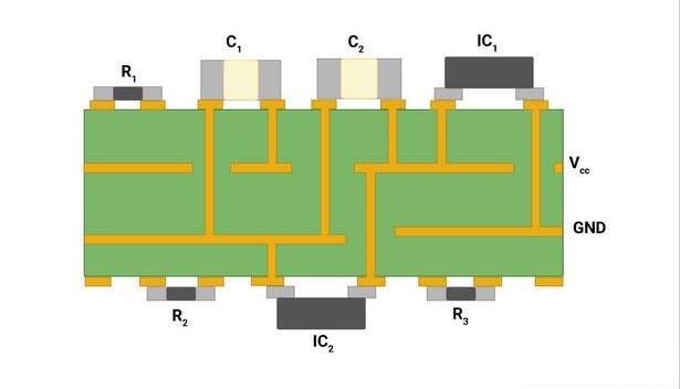
In high-frequency PCB design, power and ground are often implemented using dedicated planes rather than long bus structures.
A plane-based power distribution network can provide a lower-impedance path and a more predictable current-return structure.
A continuous reference plane also provides a return-current path for high-speed signals. This reduces loop area and helps minimize electromagnetic radiation.
This is an important difference between high-frequency and low-frequency PCB design. At high frequencies, return-current paths should be considered as carefully as signal traces themselves.
1.2 Optimize Through-Hole and Via Structures
Through-holes and vias require clearances in power and ground planes. If the clearance around a via is unnecessarily large, it can interrupt the reference plane and force the signal return current to take a longer path.
This may increase:
- Current-loop area
- Parasitic inductance
- Electromagnetic radiation
- Local impedance discontinuity
- Crosstalk
If several high-speed signal traces pass near a large plane clearance, they may also share portions of the same return path, creating common-impedance coupling.
For this reason, via clearances should be designed according to the actual manufacturing and electrical requirements rather than made unnecessarily large.
1.3 Provide an Appropriate Return Path for Every Signal
Every high-speed signal requires a complete current-return path.
The signal and its return current form a loop. The smaller this loop area is, the lower the associated inductance and electromagnetic radiation generally become.
Therefore, high-speed traces should be routed close to a continuous reference plane whenever possible.
A signal should not be viewed as a single trace. Instead, the complete structure should be considered:
Signal trace + dielectric + reference plane + return current
This concept is fundamental to signal integrity.
1.4 Separate Sensitive Analog and Digital Power Domains
High-frequency analog circuits, RF circuits, and sensitive clock or PLL circuits may be particularly susceptible to digital switching noise.
Analog and digital power domains should therefore be carefully managed according to the system architecture.
Rather than automatically splitting every power plane, designers should determine where separation is electrically beneficial and ensure that signal-return paths remain continuous.
If a high-speed signal crosses a split or discontinuity in its reference plane, its return current may be forced to detour around the discontinuity, increasing loop area and EMI.
1.5 Isolate Noise-Sensitive Components
Noise-sensitive components such as PLLs, oscillators, RF front ends, ADCs, and low-noise analog circuits should be physically separated from strong digital-noise sources whenever possible.
Recommended practices include:
- Keep noisy switching circuits away from sensitive analog circuits.
- Provide short and direct power-return paths.
- Use appropriate decoupling capacitors.
- Avoid routing high-speed clocks through sensitive analog areas.
- Maintain a continuous reference plane.
1.6 Avoid Unnecessary Power-Plane Overlap
Overlapping power planes can create parasitic capacitance between adjacent layers.
At high frequencies, this capacitance can provide an unintended coupling path for high-frequency noise.
Power-plane structures should therefore be evaluated as part of the complete stack-up rather than considered independently.
2. Transmission Line Interference
In high-speed PCB systems, traces behave as transmission lines when their electrical length becomes significant relative to the signal rise time.
Common PCB transmission-line structures include:
- Microstrip
- Stripline
- Coplanar waveguide
One of the most important problems associated with transmission lines is signal reflection.
When a signal encounters an impedance discontinuity, part of its energy may be reflected toward the source.
2.1 Effects of Signal Reflection
Signal reflection can cause:
- Overshoot
- Undershoot
- Ringing
- Timing errors
- Waveform distortion
- Reduced noise margin
- Increased electromagnetic emissions
The reflected signal may combine with the original signal, making the waveform more difficult for the receiver to interpret.
Therefore, impedance matching is an important part of high-speed PCB design.
2.2 Control Transmission-Line Impedance
The most effective way to reduce reflection is to maintain a controlled and consistent transmission-line impedance.
Important parameters include:
- Trace width
- Trace thickness
- Dielectric thickness
- Dielectric constant (Dk)
- Reference-plane distance
- Via structure
- Connector geometry
The PCB stack-up should be defined before final routing so that the required impedance can be achieved consistently.
2.3 Avoid Abrupt Impedance Discontinuities
Designers should minimize unnecessary impedance discontinuities caused by:
- Sharp corners
- Excessive vias
- Sudden trace-width changes
- Large component pads
- Connectors
- Plane discontinuities
For high-speed routing, 45-degree corners or curved traces are generally preferred over unnecessary 90-degree corners.
The number of vias should also be minimized where practical because every via introduces a change in the transmission-line structure.
When a signal changes PCB layers, designers should provide an appropriate return-current path near the via transition.
2.4 Minimize Unnecessary Stubs
A stub is an unused branch connected to a transmission line.
When the stub is electrically short, its effect may be limited. As its electrical length increases, however, it can introduce reflections and resonances.
This is particularly important for high-speed interfaces with fast edge rates.
Where possible, designers should use:
- Back-drilling
- Blind or buried vias
- Proper via transitions
- Optimized routing
to reduce the effective stub length.
3. PCB Coupling and Crosstalk
PCB coupling occurs when unwanted electrical or electromagnetic energy from one circuit is transferred to another circuit.
Common coupling mechanisms include:
- Common-impedance coupling
- Common-mode field coupling
- Differential-mode coupling
- Capacitive coupling
- Inductive coupling
- Power-line coupling
- Trace-to-trace crosstalk
Understanding these mechanisms is essential for controlling PCB crosstalk and maintaining signal integrity.
3.1 Common-Impedance Coupling
Common-impedance coupling occurs when an interference source and a victim circuit share part of the same conductive path.
Examples include:
- Power distribution networks
- Ground paths
- Shared buses
- Common return paths
When current flows through a shared impedance, it produces a voltage:
V = I × Z
This unwanted voltage can appear on the victim circuit and interfere with its operation.
Reducing shared impedance and providing independent return paths are effective methods for controlling common-impedance coupling.
3.2 Common-Mode Field Coupling
A changing electromagnetic field can induce unwanted voltage in a PCB loop.
For magnetic-field coupling, the induced voltage is related to the rate of change of magnetic flux and the effective loop area.
A simplified relationship is:
V_induced ∝ A × dB/dt
where:
- A = effective loop area
- B = magnetic flux density
- dB/dt = rate of change of magnetic flux density
This demonstrates an important PCB design principle:
Smaller loop area generally means lower susceptibility to magnetic-field coupling.
Therefore, high-speed signal paths and their return paths should be kept close together.
3.3 Differential-Mode Field Coupling
Differential-mode coupling occurs when electromagnetic energy couples directly into a pair of conductors or another circuit structure.
Keeping paired conductors close together reduces the effective loop area and can improve immunity to external electromagnetic fields.
This is one reason why differential signaling is widely used in high-speed communication interfaces.
For differential pairs, designers should maintain:
- Consistent spacing
- Similar trace lengths where required
- Continuous reference planes
- Controlled differential impedance
- Symmetrical routing where practical
3.4 Trace-to-Trace Crosstalk
PCB crosstalk occurs when energy from one signal trace couples into a nearby signal trace.
Two major mechanisms are:
Capacitive crosstalk: caused primarily by electric-field coupling through parasitic capacitance.
Inductive crosstalk: caused primarily by magnetic-field coupling associated with changing current.
Crosstalk becomes more severe when:
- Traces are routed too closely
- Parallel routing is excessive
- Signal edges are very fast
- Trace spacing is insufficient
- Return paths are discontinuous
- High-voltage or high-current switching signals are nearby
3.5 Methods to Reduce Crosstalk
Several methods can be used to reduce PCB crosstalk.
Increase Trace Spacing
Increasing the distance between adjacent signal traces reduces electromagnetic coupling.
Where PCB space permits, sensitive high-speed signals should be separated from aggressive switching signals.
Use Ground Structures Carefully
A grounded guard trace can sometimes reduce coupling between adjacent signals. However, its effectiveness depends on the complete geometry and return-current structure.
If a guard trace is used, it should be connected to the reference plane with sufficiently frequent vias.
Reduce Parallel Routing
Long parallel sections increase coupling. Designers should minimize unnecessary parallel routing between noisy and sensitive signals.
Reduce Loop Area
For inductive coupling, reducing the loop area of the aggressor and victim circuits can significantly reduce interference.
Avoid Shared Return Paths
Signals with substantially different noise characteristics should not unnecessarily share the same return path.
3.6 Signal Termination and Signal Integrity
Proper termination can reduce reflections and improve signal integrity.
Depending on the interface, designers may use:
- Series termination
- Parallel termination
- Thevenin termination
- AC termination
- Differential termination
The appropriate termination method depends on driver characteristics, transmission-line impedance, signal speed, topology, and receiver requirements.
For dense interconnect systems, the PCB layout itself can be designed as part of the controlled transmission path.
4. EMI Interference
As operating speeds increase, EMI interference becomes increasingly difficult to control.
High-speed circuits generate rapidly changing voltage and current signals. These signals can create electric and magnetic fields that couple into nearby circuits or radiate from the PCB.
Sensitive high-speed receivers may detect interference that slower circuits would effectively ignore.
4.1 Reduce Current Loop Area
Every current loop can behave as an electromagnetic radiator.
Therefore, designers should minimize:
- Number of unnecessary loops
- Loop area
- Return-path discontinuities
- Long signal-return paths
A continuous reference plane is one of the most effective structures for maintaining a compact return path.
Whenever possible, the signal and its return current should remain physically close.
4.2 Use Filtering
Filtering can reduce conducted noise on both power and signal interfaces.
Common techniques include:
- Decoupling capacitors
- EMI filters
- Ferrite components
- Common-mode chokes
- LC filters
The filter should be placed as close as practical to the noise source or the interface being protected.
4.3 Apply Appropriate Shielding
Shielding can reduce electromagnetic coupling between sensitive circuits and external noise sources.
Possible shielding structures include:
- Metal shields
- Shield cans
- Conductive enclosures
- Grounded shielding structures
- PCB via fences
However, shielding should complement good PCB layout rather than replace it.
A poorly designed return path can still produce EMI even when a shield is present.
4.4 Control High-Frequency Switching Activity
Reducing unnecessary switching activity can help lower EMI.
Designers can consider:
- Reducing unnecessarily fast edge rates
- Optimizing clock routing
- Controlling switching-node areas
- Using appropriate slew-rate control
- Separating noisy and sensitive circuits
The goal is not simply to make a circuit slower, but to use an edge rate appropriate for the actual system requirements.
4.5 Optimize PCB Dielectric Structure
The dielectric structure of a PCB affects both impedance and electromagnetic behavior.
Increasing the distance between a signal trace and its reference plane generally changes the field distribution and transmission-line impedance.
For high-frequency applications, designers should carefully control:
- Dielectric thickness
- Dk
- Df
- Copper roughness
- Trace geometry
- Reference-plane spacing
For demanding RF and microwave applications, specialized low-loss materials may be required.
5. Key Principles of High-Frequency PCB Design
A successful high-frequency PCB design should follow several fundamental principles.
5.1 Maintain Stable Power and Ground
Power distribution and grounding should provide low-impedance paths for both power currents and high-frequency return currents.
5.2 Maintain Controlled Impedance
Transmission lines should be designed with predictable characteristic impedance, and impedance discontinuities should be minimized.
5.3 Provide Continuous Return Paths
A signal trace without a suitable return path can create a large current loop and increase EMI and crosstalk.
5.4 Minimize Coupling
Increase spacing between sensitive and aggressive signals, reduce parallel routing, and control common return paths.
5.5 Control EMI
Use appropriate grounding, filtering, shielding, stack-up design, and routing techniques to satisfy EMC requirements.
6. High-Frequency PCB Manufacturing Considerations
Good high-frequency performance depends not only on PCB layout but also on manufacturing accuracy.
Important manufacturing parameters include:
- Trace width and spacing
- Copper thickness
- Dielectric thickness
- Material Dk and Df
- Layer registration
- Via dimensions
- Via-to-plane clearance
- Surface finish
- Copper surface roughness
- Controlled impedance
Even a small variation in dielectric thickness or trace geometry can change the actual impedance of a transmission line.
Therefore, PCB designers should provide the fabricator with clear stack-up and impedance requirements before production.
Kingda can support high-frequency and high-speed PCB manufacturing by coordinating material selection, stack-up construction, controlled impedance, trace geometry, via structures, and manufacturing process control.
Conclusion
In modern high-speed electronics, high-frequency PCB design requires much more than simply routing signals between components.
Engineers must consider PCB power noise, transmission-line behavior, PCB coupling, PCB crosstalk, impedance discontinuities, return-current paths, and EMI interference as part of the complete electrical system.
The most effective approach is to control these factors from the earliest stages of stack-up planning and PCB layout. Stable power and ground structures, continuous return paths, controlled impedance, appropriate termination, optimized routing, reduced loop area, and suitable PCB materials can significantly improve signal integrity and electromagnetic compatibility.
With accurate manufacturing and appropriate process control, Kingda can help support reliable PCB production for high-speed digital, RF, microwave, telecommunications, automotive electronics, and other demanding applications.