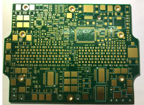
As electronic products continue to become smaller, faster, and more highly integrated, the demand for advanced multilayer PCB technology is increasing rapidly. Modern electronic devices commonly use BGA packages, high-density routing, fine-pitch components, and increasingly complex interconnections. These requirements place greater demands on PCB manufacturing accuracy, electrical testing, via technology, material selection, and production efficiency.
A reliable PCB manufacturing process must therefore combine advanced equipment, experienced engineering teams, precise process control, and comprehensive electrical testing.
This article introduces key aspects of multilayer PCB production, including PCB testing, test-point generation, via structures, HDI technology, manufacturing capabilities, and production lead times.
1. Multilayer PCB Manufacturing and Product Capabilities
Modern PCB manufacturing requires a combination of advanced production equipment, process engineering, and strict quality control.
Kingda provides PCB manufacturing capabilities covering a wide range of board structures and applications, including:
- 1–32 layer multilayer PCB
- High-Tg PCB
- Thick copper PCB
- Rigid-flex PCB
- High-frequency PCB
- Mixed-dielectric multilayer PCB
- Blind and buried via PCB
- Metal-core PCB
- Halogen-free PCB
- HDI PCB
Different PCB structures require different manufacturing processes and quality-control methods. For example, high-frequency PCBs require tighter control of dielectric properties and impedance, while thick copper PCBs require specialized copper plating and thermal process control.
For multilayer boards, layer registration, lamination, drilling, plating, etching, and electrical testing are especially important.
2. Why PCB Testing Is Essential
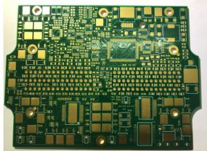
Finished-board inspection is an important part of the PCB manufacturing process.
For a completed multilayer PCB, electrical testing is generally performed to identify defects such as:
- Open circuits
- Short circuits
- Unwanted electrical connections
- Excessive conductor loss
- Manufacturing-related connection defects
Visual inspection and automated optical inspection (AOI) can identify many physical defects, but electrical testing is required to verify whether the finished board actually satisfies its electrical connectivity requirements.
The testing process generally includes:
- Establishing the required test points
- Generating test-point data
- Preparing the appropriate test fixture or probing system
- Connecting the PCB to the testing equipment
- Performing continuity and isolation tests
- Recording and analyzing test results
- Reworking or rejecting boards that fail the defined criteria
Electrical testing becomes increasingly important as PCB density increases.
3. PCB Test-Point Generation
Test-point generation is one of the critical steps in automated PCB testing.
Traditionally, test points for single-sided, double-sided, and through-hole multilayer boards could often be identified manually. When a PCB contained relatively few pads and simple routing, this approach was practical.
However, modern electronic products have significantly higher component density and much more complicated routing.
Several factors make manual test-point generation increasingly difficult:
- Smaller component packages
- BGA and fine-pitch devices
- Higher routing density
- More PCB layers
- Smaller pads
- HDI structures
- Shorter product development cycles
- More small-batch and high-mix production
- Higher requirements for manufacturing efficiency
As PCB complexity increases, manually selecting test points becomes time-consuming and more susceptible to errors.
Automated test-point generation and computer-aided testing can significantly improve efficiency and consistency.
3.1 Test Coverage and Accessibility
Not every electrical node can necessarily be accessed directly by a conventional test probe.
Therefore, test-point planning should consider:
- Test-point accessibility
- Pad size
- Component clearance
- Probe spacing
- Board thickness
- PCB surface components
- BGA regions
- Via accessibility
- Required electrical test coverage
For high-density boards, designers should consider testability during the PCB layout stage rather than waiting until production.
Design-for-Testability (DFT) can make electrical testing faster, more reliable, and more cost-effective.
4. The Increasing Complexity of Multilayer PCBs
As electronic component integration continues to increase, component packages are becoming smaller and PCB routing density is becoming higher.
BGA packages are now widely used in many applications because they provide a large number of interconnections within a relatively small footprint.
As a result, multilayer PCB designs increasingly use:
- Fine traces
- Small vias
- Microvias
- Blind vias
- Buried vias
- High layer counts
- High-density interconnect structures
Reducing trace width and spacing allows more circuits to fit within the same board area, while increasing the number of PCB layers provides additional routing space.
Advanced PCB designs may require extremely fine line widths and spaces, depending on the application, material, PCB fabricator, and HDI process capability.
The actual manufacturable geometry should always be confirmed with the PCB manufacturer before design release.
5. PCB Vias and Their Functions
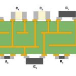
A PCB via is a conductive connection used to electrically connect different layers of a PCB.
Vias have two primary functions:
- Electrical interconnection between PCB layers
- Component or structure-related connection and routing support
In multilayer PCB production, via structures are generally classified into three main types:
- Through vias
- Blind vias
- Buried vias
These structures provide different routing capabilities and are selected according to the PCB stack-up and design requirements.
6. Through Vias
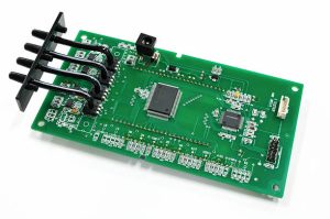
A through via extends through the entire PCB and can connect multiple conductive layers.
It is one of the simplest and most widely used types of PCB vias.
Advantages include:
- Relatively simple manufacturing
- Lower manufacturing complexity
- Good reliability
- Suitable for many conventional multilayer PCBs
However, through vias occupy routing space on every layer they pass through. As PCB density increases, this can limit routing flexibility.
For high-density designs, blind and buried via structures may provide more efficient use of available routing space.
7. Blind Vias
A blind via connects an outer PCB layer to one or more internal layers but does not extend through the entire board.
For example, a blind via may connect the top layer to an internal signal layer.
Blind vias are especially useful in HDI PCB designs because they can:
- Increase routing density
- Save surface area
- Improve component fan-out
- Support fine-pitch BGA routing
- Reduce unnecessary through-hole structures
The depth and diameter of a blind via must be controlled according to the PCB fabrication process.
The allowable aspect ratio, drilling method, copper plating requirements, and material structure all influence manufacturability.
8. Buried Vias
A buried via connects internal PCB layers without extending to the outer surface of the board.
Because it is completely enclosed within the multilayer structure, it cannot normally be accessed directly from the PCB surface.
Buried vias can provide additional routing flexibility in complex multilayer designs.
They are particularly useful when designers need to connect internal signal layers while preserving outer-layer routing space.
However, buried vias require additional manufacturing steps and can increase PCB production complexity and cost.
9. Blind and Buried Vias in HDI PCB Manufacturing
HDI PCB technology combines fine lines, microvias, high-density routing, and advanced layer interconnection structures.
Microvias are typically created using laser drilling and are much smaller than conventional mechanically drilled vias.
HDI structures may use:
- Laser microvias
- Blind vias
- Buried vias
- Stacked microvias
- Staggered microvias
- Via-in-pad structures
These technologies allow designers to route more connections within limited PCB space.
However, HDI manufacturing requires precise control of:
- Laser drilling
- Registration accuracy
- Copper plating
- Lamination
- Dielectric thickness
- Microvia dimensions
- Via-to-pad alignment
- Layer-to-layer alignment
Therefore, successful HDI production depends heavily on manufacturing process capability.
10. PCB Drilling and Manufacturing Cost
Drilling is an important manufacturing process for multilayer boards because holes and vias are required for both electrical interconnection and mechanical functions.
The overall cost contribution of drilling depends on:
- Number of holes
- Hole diameter
- Board thickness
- Material type
- Aspect ratio
- Via technology
- Drilling method
- Production volume
- Required tolerance
Conventional through-hole drilling is generally simpler than HDI laser drilling or complex sequential lamination structures.
For this reason, via structure should be selected according to actual electrical requirements rather than using the most complex structure by default.
11. PCB Manufacturing Quality Control
Reliable PCB manufacturing requires quality control throughout the complete production process rather than relying only on final inspection.
Important control points include:
Material Inspection
PCB laminates, copper foil, prepreg, and other materials should meet the specified electrical, thermal, and mechanical requirements.
Lamination Control
Multilayer boards require precise control of temperature, pressure, time, and dielectric thickness during lamination.
Registration Control
Accurate layer-to-layer alignment is essential for fine-line and HDI structures.
Etching Control
Trace width and spacing must remain within the specified manufacturing tolerance.
Drilling Control
Hole diameter, hole position, depth, and aspect ratio must meet design requirements.
Plating Control
Copper thickness and plating uniformity directly affect electrical performance and reliability.
Electrical Testing
Finished boards should undergo appropriate electrical testing to identify open and short circuits and verify connectivity.
12. PCB Production Lead Time
Production lead time depends on PCB structure, layer count, material, technology, quantity, surface finish, testing requirements, and production capacity.
As a general reference, typical lead times may vary as follows:
- Simple single- and double-sided prototype boards: approximately 6–7 working days
- 4–8 layer boards: approximately 9–12 working days
- 10–16 layer boards: approximately 15–20 working days
- HDI boards: approximately 20 working days or more
Fast-turnaround services may be available for certain prototypes and simple double-sided boards, depending on design complexity and production capacity.
Actual delivery schedules should be confirmed based on the final Gerber files, stack-up, material requirements, quantity, and testing specifications.
13. How to Improve Multilayer PCB Manufacturing Efficiency
As PCB designs become more complex, manufacturers can improve production efficiency through better engineering coordination and process automation.
Important strategies include:
- Automated test-point generation
- Automated optical inspection
- Automated electrical testing
- Advanced drilling equipment
- Laser drilling for HDI structures
- Automated material handling
- Process data management
- Manufacturing traceability
- Standardized engineering review
Designers can also improve manufacturing efficiency by following Design for Manufacturing (DFM) principles.
Before production, the PCB design should be reviewed for:
- Minimum trace width and spacing
- Minimum hole size
- Via structure
- Aspect ratio
- Copper thickness
- Layer registration
- Solder mask clearance
- Component density
- Test-point accessibility
Early DFM analysis can identify potential manufacturing problems before they result in production delays.
14. Kingda’s Multilayer PCB Manufacturing Capabilities
Kingda supports a broad range of PCB manufacturing requirements, including conventional multilayer boards, high-Tg PCBs, thick copper boards, high-frequency PCBs, rigid-flex PCBs, metal-core PCBs, halogen-free boards, and advanced HDI structures.
For complex multilayer PCB projects, Kingda can integrate engineering review, material selection, stack-up planning, drilling, lamination, plating, inspection, and electrical testing into a controlled manufacturing process.
This integrated approach helps improve consistency and supports demanding applications where PCB reliability, dimensional accuracy, and electrical performance are critical.
Conclusion
The increasing integration of electronic components is driving PCB technology toward higher layer counts, finer traces, smaller vias, and more sophisticated interconnection structures.
A reliable multilayer PCB requires more than simply adding additional layers. PCB manufacturers must carefully control material selection, lamination, registration, etching, drilling, plating, inspection, and PCB testing.
At the same time, PCB vias, including through vias, blind vias, and buried vias, play an increasingly important role in high-density routing and HDI PCB manufacturing.
By combining advanced manufacturing equipment, automated testing, experienced engineering teams, DFM analysis, and strict process control, Kingda can support the production of high-quality multilayer PCBs for demanding electronic applications.