
Preventing Tombstoning and Cold Joints at the Design Stage
When a chip component stands up on one end after reflow, or a joint that looks complete turns out to be electrically open, the first suspects are usually the paste, the profile or the placement machine. Production data points somewhere else: a large share of these defects can be traced back to how the pads, the copper and the solder mask were drawn. Both failures have clear physical causes, and both can be designed out before a single board is built.
Why the Design Decides
Tombstoning is a surface tension event. The alloy at one termination melts before the other, the molten end wets and pulls, and the component rotates up onto its end. The root cause is always an imbalance between the two ends: unequal heat, unequal paste volume or unequal wetting.
A cold solder joint is a metallurgical shortfall. The alloy did not fully melt, or the surfaces were not clean enough to wet, so no proper intermetallic layer formed and the connection exists only in appearance.
Both are usually created long before the reflow oven. Pad geometry, copper distribution and solder mask apertures set how much paste lands on each pad, how fast each end of the component heats, and how much the solder is free to spread. A design that leaves the two ends unequal has handed the process a problem it can only partly correct.
Pad Symmetry Comes First
For chip components the pads must be mirror images of each other: the same width, the same length, the same solder mask relationship and, as far as possible, the same connection to the rest of the board.
Even a small difference matters at small package sizes. On a 0402 or 0201 part, a tenth of a millimetre of difference in pad length changes the amount of paste on one end enough to shift the balance of forces at reflow.
The safest starting point is the manufacturer’s recommended land pattern, or the standard IPC land pattern calculation, rather than a pattern carried over from an older design. Differences that are invisible at 0603 become decisive two package sizes smaller.
Pad Size: Larger Is Not Safer
There is a persistent instinct that a bigger pad is easier to solder. It is not, and it can make both defects more likely.
Too small a pad holds too little paste. The fillet that forms is thin, wetting is incomplete, and the joint may be marginal or open. Too large a pad holds too much paste, which produces a larger molten volume and a stronger pull during reflow: the same force that forms a good fillet on a correct pad becomes a force large enough to lift a small component.
The working rule is a modest extension beyond the component termination on each side and a slight increase in width over the component body, keeping the inner gap between the two pads wide enough to prevent bridging on the smallest packages in the design.
Thermal Balance and Copper
The most common and least obvious cause of tombstoning is an asymmetry in heat. One pad connects to a ground plane or a power pour; the other connects to a thin signal trace. The pad on copper draws heat away and comes up to temperature slowly, while the pad on the trace heats quickly. Its paste melts first, and the pull begins.
This is why copper geometry should be reviewed for symmetry across every two-terminal passive, not just for electrical function. A track that has to be wide for current reasons can be balanced by widening the connection at the other pad, or by examining whether the layout can place the passives so that both ends see comparable copper.
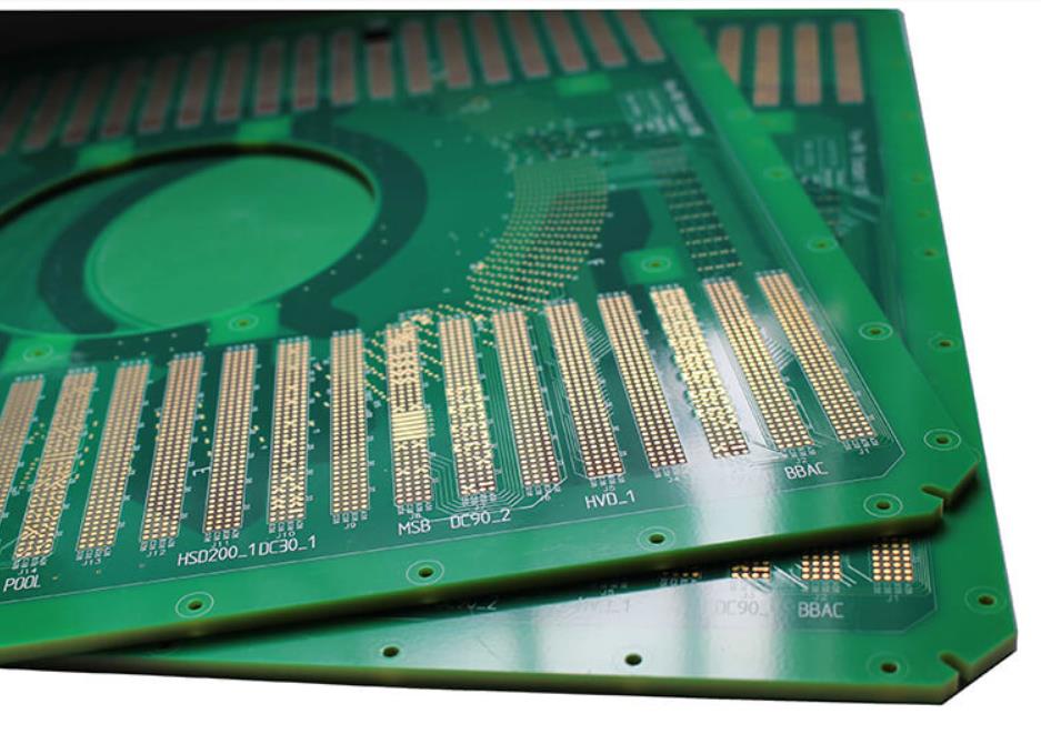
Where a pad must connect to a large pour, the connection should be made through a thermal relief: several narrow spokes rather than a solid connection. The spokes carry the current while restricting the rate at which heat leaves the pad, so both ends of the component approach the liquidus at similar times. The width of the traces leaving the two pads should also be kept similar for the same reason.
Placement and Thermal Shadowing
Component placement influences the temperature each joint actually sees. Large bodies absorb and radiate heat differently from small ones, and a tall device standing upstream of the airflow casts a thermal shadow over the parts behind it. Small passives sitting in that shadow region may not reach the liquidus while everything around them does.
The design countermeasures are spacing rules: keep small passives away from the immediate vicinity of high-mass devices such as large packages, power inductors and heatsinks; avoid clustering all the small parts in one dense region; and, where an assembly has devices of very different thermal mass, distribute them so the board heats more evenly.
Dense routing has a related effect. Regions of tightly packed copper and vias are thermally heavy, and a component placed there heats more slowly than the same component on an open area of the board.
Solder Mask Openings for a Cold Solder Joint
Solder mask defines where the solder is allowed to spread. If the opening is wrong, the joint suffers.
An opening that is too small leaves mask encroaching on the land, reducing the usable pad area and the paste volume that can be deposited. An opening that is too large lets the alloy flow onto the mask-free laminate beside the pad, where it does not form a useful fillet and leaves the joint short of material. Both produce marginal joints, and the second produces them intermittently, which makes the cause harder to find.
The web of mask between adjacent pads matters just as much. As pitches shrink the web becomes thin, and a web that is too narrow may not survive the process, allowing solder to travel between pads during reflow. Where the design is close to that limit, a non-solder-mask-defined pad, in which the copper defines the land and the mask opening is larger than the pad, gives more predictable results than a mask-defined one.
Shadowing and Test Access
Two layout habits reduce the later difficulty. Keep components that must be inspected or probed clear of obstructions, since a test pad hidden under a connector body or a tall component cannot be reached and may also be missed by optical inspection. And keep clearance around components that need rework, because a part surrounded on all sides by taller parts is difficult to remove and replace without disturbing its neighbours.
Design and Process Have to Agree
A good layout still depends on a process that matches it. Two process settings matter especially for these defects: the ramp rate into reflow, which if too fast can melt one end of a component before the other has begun to heat, and the peak temperature and time above liquidus, which if too low leaves joints that look formed but are not fully wetted.
Stencil apertures are the other half of the agreement. Reducing the paste volume slightly on small chip components, or changing the aperture shape to reduce the deposited volume on each end, is a common correction for tombstoning. Where a design and its stencil apertures are being prepared together, that correction is free rather than a second iteration.
The audit that catches these issues is a design review that treats manufacturability as a deliverable rather than a courtesy, run before the files are released for fabrication. Our layout quality checklist covers the items to check, the DFM review describes how the findings are handled before production, and the defects that still reach the line are covered in the guide to common soldering defects.
<img src="https://www.gopcba.com/wp-content/uploads/2026/08/pl149813980-oem_fast_turn_custom_pcb_rigid_enig_printed_circuit_board_quick_turn.webp" alt="thermal relief spokes connecting a pad to a copper pour” />
FAQ
Which single design change prevents most tombstoning? Symmetric copper at both terminations, connected through thermal relief where a pad joins a plane. Heat balance between the two pads matters more than any other factor.
Are oversized pads a safe margin? No. Excess paste increases the surface tension available to lift a small component, and large pads raise the risk of bridging between adjacent terminations.
Can a design fault be corrected at the stencil? Sometimes, by reducing paste volume on the vulnerable pads. It is a useful compensating control, but it does not fix an unbalanced layout.