



HDI Layout: Shrinkage Compensation and Microvia Rules
High density interconnect changes the questions a layout has to answer. On a conventional board the constraint is usually space: how to fit the routing into the area available. On an HDI board the constraint becomes agreement — between the stack-up and the drill programme, between the artwork and the way the laminate moves when it is pressed, and between the design rules and what the fabricator can actually hold on a panel that has been through several lamination cycles.
What follows are the practical points that decide whether an HDI layout turns into a buildable board or into a series of queries.
Stack-Up and Material
The stack-up is where HDI is decided. Three things have to be settled together: the laminate, the layer construction and the copper.
Low-loss materials are usual at this density because the traces are fine and the signals are fast, and the permittivity has to be stable enough that impedance control means something. The loss behaviour matters less for its own sake than for whether the design can hold the insertion loss budget across the routes it has.
The construction matters for flatness as much as for electrical function. Symmetry about the centre line keeps the panel from warping during pressing, and the choice between one, two or three build-up layers on each side of the core determines how many laser drilling cycles the board requires and how deep each of them goes. That decision has to be taken with the fabricator, because the achievable laser depth and the copper thickness at each level are process properties rather than design preferences.
Copper foil selection is often overlooked on HDI. Finer traces are etched more accurately in a low-profile foil, and the same choice improves the loss of the finished trace because the current is not forced through a rough surface. The trade is cost and availability, and it is worth settling early rather than discovering it at quotation.
Microvia and Blind Via Rules
The structures that make HDI possible are the small vias that connect only the layers they need to.
Laser-drilled vias are produced in a limited range of diameters, and the depth is limited by the process rather than by the design. A common rule is that a microvia should not be deeper than roughly its own diameter, which in practice means it spans the outer layer and the one beneath it. Deeper structures are built by stacking or staggering rather than by drilling further.
That gives the two standard arrangements. A stacked via places one microvia directly on top of another, which conserves routing space and produces the shortest vertical path. It requires the lower via to be filled and planarised so that the next one lands on a flat copper surface, which adds operations and cost. A staggered arrangement offsets each via from the one below so that the drilling does not coincide, which avoids the fill process but consumes routing area because the offset region cannot be used freely.
Both arrangements have to be captured in the design rules, since the layout software needs to know which layers each microvia type may span and what clearance the offset requires.
Via in Pad for Fine-Pitch Arrays
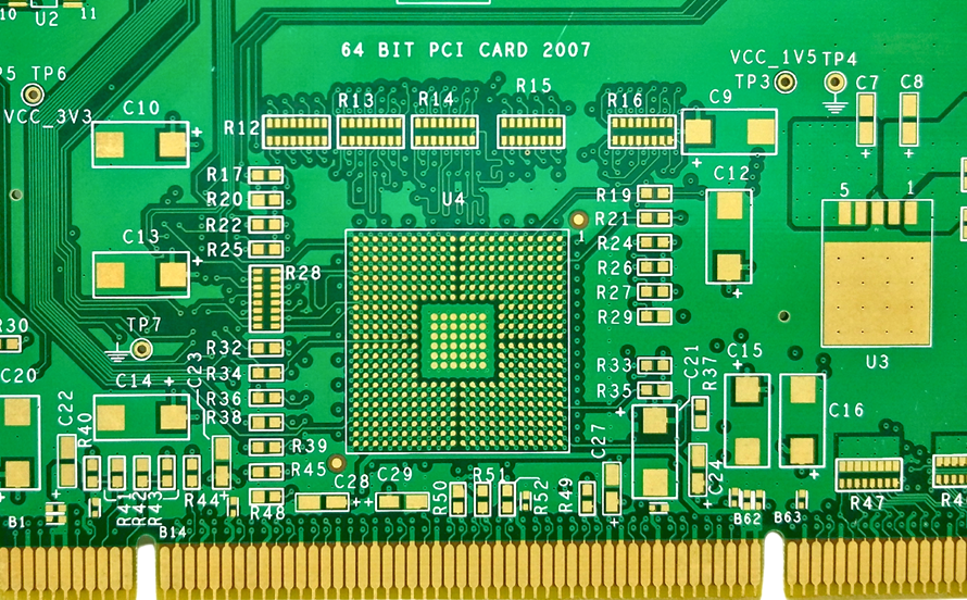
Escaping a fine-pitch ball grid array usually requires the via to sit inside the pad rather than beside it, because there is not enough room in the channel between pads for both a route and a via.
A via placed in a pad creates a specific risk: the barrel is open at the pad surface, and during reflow the solder can wick down into it, leaving the joint short of material. The countermeasure is to fill the via with resin and cap it with copper so the pad surface is flat and closed, which is what makes the process reliable. It is also what makes it more expensive, and the requirement should be stated explicitly rather than left to the fabricator to infer.
The details are covered further in the note on via in pad for fine-pitch BGA.

Routing and Impedance
Fine traces change the arithmetic of familiar rules. The spacing that keeps crosstalk within budget is a multiple of trace width, and when the width falls the absolute spacing falls with it, which is why densely routed HDI layers can look compliant while carrying more coupling than expected.
Reference plane continuity deserves particular attention because the very vias that save space are what breaks it. When a microvia interrupts the reference plane a signal was returning through, the return current has to find another path, and the resulting loop is a source of both radiation and loss. The standard remedy is to place return vias adjacent to the signal via, tying the two reference planes together close to the transition, with spacing related to the highest frequency the design carries.
Where the planes are split, as they often are on a dense HDI board, stitching capacitors placed across the split give the return current a local path between the two planes. The spacing is again a function of frequency: the closer they are placed, the higher the frequency at which the arrangement still works.
Lamination Shrinkage: The Variable Nobody Draws
The most common cause of an HDI board that works in simulation and fails in production is movement during lamination.
Core and prepreg do not shrink by the same amount, and their shrinkage is not the same in both directions. A length of laminate that leaves the press slightly shorter than it went in will take every via with it, and because the movement is a proportion rather than an offset, the error is larger at the far end of the panel than near the registration point. On a design with several build-up layers, that movement accumulates over successive press cycles.
Three practices address it. The first is to compensate the artwork by a scale factor derived from the fabricator’s history with that material and construction, so that the pattern is drawn slightly oversize and lands on target after pressing. The second is to place non-functional via patterns at the panel edge where the measurement equipment can use them to confirm the actual movement of the lot. The third is to sequence the drilling so that laser-drilled microvias are produced before mechanical drilling, since mechanical drilling through a stack that already contains fine laser structures is a risk to those structures rather than the other way round.
The number to keep in mind is that laser drilling itself can be accurate to a small fraction of a thousandth of an inch and still produce a board whose total registration error after pressing is several times that, because the press moves everything.
What the Fabricator Needs to See in the Data
Two minimum features determine whether a design is manufacturable at all: the width of the ring around each laser-drilled via, and the minimum trace width and spacing on each layer. Both have to match the fabricator’s capability rather than the design’s aspiration, because a ring that is too narrow will be trimmed to make the board producible, and a trace that is too fine will simply change width after etching and take the impedance with it.
Test access needs planning too. On a dense board there is often no room for probe pads on the outer layers, so test points are placed on inner layers and reached through the build-up, which works but has to be arranged while the stack-up is still open.
Impedance verification is handled with coupons built into the panel rather than with the product routing, which means the coupon geometry has to be specified in the fabrication data and its tolerance agreed in advance.
An Escape That Works
A representative fine-pitch case is a ball array at the smallest pitch in common production use, on a board with four build-up layers. The escape runs from the pad to a laser via of the smallest diameter the process offers, and out to a trace at the finest width the layer supports, with the transition from pad to trace shaped so that the impedance change is gradual rather than abrupt.
Verification then happens in two places: the signal path is checked for reflection across the band of interest, and the supply arrangement is checked against its impedance target, with the decoupling components placed close enough to the device that their distance does not dominate. Both checks are on the same layout, and both are easier to satisfy when the escape is planned before the rest of the routing rather than after it.
Common failures on this kind of board are consistent: microvias that were not filled and produce voids during soldering; vias placed in pads without the fill and cap that make them safe; rings too narrow to survive etching; shrinkage not compensated so that laser vias miss their targets after pressing; and reference planes broken without return vias, which is discovered later as an emissions problem. Each is cheap to prevent at layout and expensive to diagnose afterwards.
Where these structures sit within the fabrication process is described in the note on HDI blind via fabrication, and the review that catches the rest is set out in the layout quality checklist.

FAQ
Are stacked vias always better than staggered ones? Stacked vias save space and shorten the path, but require filling and planarising the via beneath, which adds process steps. Staggered vias avoid that at the cost of routing area.
Why does a via in a pad need filling? Because an open barrel under a pad lets solder wick away from the joint during reflow. Filling it with resin and capping it with copper closes the surface.
How much does lamination move the pattern? It depends on material and construction, but the movement accumulates across press cycles and is proportionally larger further from the registration point. It is compensated by scaling the artwork before imaging.



2 Comments
Smallest Components to Shrink PCB Area
[…] The fourth is thermal. A package with almost no surface area cannot dissipate much heat, so power handling has to be decided by thermal path rather than by package rating — typically through thermal vias into copper, which is itself a layout decision with area cost. The practices involved are described in this review of HDI layout and microvia rules. […]
HDI Board CAM Data Preparation
[…] There is a geometry consequence that has to be checked. The sub-outer layer must have copper at the bottom of the laser via, which imposes a minimum spacing between blind and buried vias — four thousandths of an inch or more. Drill checks against the fabrication rules are used to find every location that violates the limit, because the requirement cannot be judged by eye across a dense board. The general structural rules that apply are covered in this review of HDI layout and microvia rules. […]