



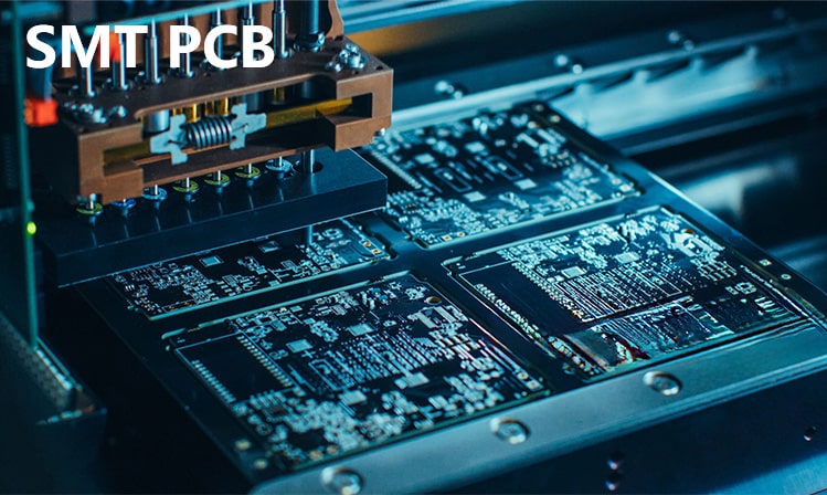
PCBA Development Process: From Requirements to Production
A printed circuit board assembly is rarely a product in itself. It is the part that makes a product function, and it sits between a set of requirements and a physical object that has to be built in quantity at a price. The work of turning the first into the second is the PCBA development process, and it succeeds or fails long before the first board is assembled. The stages below are the ones that actually gate the schedule.
Requirements Analysis Comes First
Development starts with a written statement of what the product must do and under what conditions. Function comes first: what the assembly is expected to perform, and to what accuracy and speed. A wearable device might need heart-rate monitoring, motion tracking and sleep analysis, with defined accuracy and response requirements for each. A control board might need a set of sensor inputs, a set of drive outputs and a defined response time.
The conditions are as important as the functions. The operating temperature range determines the component grades and the material choices. The enclosure determines the board dimensions and the height available for components. The power source determines the input voltage range and the efficiency target. The target market determines the regulatory standards the product must meet. And the cost target determines how much of the rest of the specification is achievable.
A requirements analysis that skips any of those items does not remove the constraint; it simply defers it until the point where it is expensive. The most common schedule failure in PCBA development is discovering, at the enclosure stage, that a component is taller than the space available or that the connector cannot be reached by a cable.
Architecture and Component Selection
The architecture stage turns the requirement list into a block diagram: a power chain, a processing element, the interfaces, the sensing and the output stages. Each block carries its own constraints, and the interfaces between them are where most of the design risk sits. The supply rails and their tolerances, the clock architecture, the data buses and the analog signal levels should all be defined at this stage rather than left to the layout.
Component selection follows the architecture and is governed by availability as much as by specification. A part that is technically ideal but has a twelve-week lead time is a schedule risk, and a part that is second-sourced is worth more to a project than a marginally better one that is not. The selection should also consider the assembly process: a package that the assembly house cannot place reliably, or one that requires a process the chosen supplier does not run, will cost more than the specification suggests.
Component selection is where the design rules that govern the physical layout are set as well, since package choices determine pad geometries and clearances. The constraints that follow from pad design are described in this article on PCB pad design standards.
Schematic, Layout and Verification
The schematic capture and the layout are the visible parts of the process, and they are usually the shortest. The verification that accompanies them is what separates a design that works from one that works reliably. Verification covers the connectivity of the netlist, the power integrity of the distribution network, the signal integrity of the fast interfaces and the thermal behaviour of the parts that dissipate power.
Some of that verification is analytical and some is empirical, and a prototype is what bridges the two. The purpose of the prototype is to test the assumptions the design made rather than to demonstrate that the circuit works, and the checks that a prototype should satisfy are described in this discussion of multilayer prototype requirements.

Design for Manufacture and Assembly Review
The DFM review is the step most often compressed when a schedule slips, and it is the step that most often prevents a costly re-spin. It examines the design from the point of view of the fabricator and the assembler: whether every feature can be produced within the process window, whether the panel can be built efficiently, whether the stencil can print the paste volumes required, and whether the placement machine can reach every component.
The review also covers the assembly sequence. Components that must be placed on both sides, parts that require a specific reflow profile, and connectors that need clearance for mating all constrain the process. Where a design contains a part that the assembler cannot handle, the correction is far cheaper at this stage than after tooling has been ordered.
Test Strategy
A test strategy determines how the assembled board will be verified, and it has to be designed rather than discovered. Electrical test of the bare board verifies continuity and isolation. In-circuit test verifies component values and solder joints. Functional test verifies that the assembly performs its function. Each of those has implications for the layout: test points, probe clearance, access to nets and the order in which tests are performed.
The test strategy also determines what happens when a board fails. A design with no diagnostic access has to be scrapped, while a design with usable test points can be diagnosed and repaired. Where a board will be produced in volume, the cost of test coverage is almost always lower than the cost of scrap.
Transition to Production
The final stage is the transfer itself: a released manufacturing package, an agreed process flow, a first article inspection and a controlled ramp. The package should include the artwork, the stackup, the fabrication and assembly drawings, the bill of materials with approved alternatives and the test programme. The ramp should be measured, with yield and defect data reviewed at each step rather than only at the end. A first article inspection is the gate that confirms the process produces what the design intended, and it should cover the geometry as well as the function, since a board that functions correctly but is built at the edge of the process window will fail later in volume.
Designers often underestimate the value of keeping the layout clean while the process runs. Because routing decisions made early constrain everything that follows, the discipline described in this discussion of escape routing pays for itself when a part has to be changed late in the programme.
FAQ
Why does the requirements stage matter so much? Because every later decision depends on it. The operating conditions set the component grades, the enclosure sets the board size and height, the market sets the standards, and the cost target sets how much of the rest is achievable. A constraint discovered late is far more expensive than the same constraint recorded at the start.
How early should the assembler be involved? Before the layout is frozen. The assembler can identify package and stencil problems, suggest placement adjustments and confirm the process window while changes are still cheap. Involving them after tooling has been ordered limits the corrections to expensive ones.
What should a manufacturing package contain? The artwork, the layer stackup, fabrication and assembly drawings, the bill of materials including approved alternatives, the test programme and the agreed acceptance criteria. Anything that affects how the board is built belongs in the package rather than in a conversation.



2 Comments
PCB Design and Production: Schematic to Volume Manufacturing
[…] on a thin board may not sit flat, and a via left open beside a pad may steal paste from the joint. PCBA development process covers the sequence from stencil to final […]
Solder Ball Placement in Small-Batch SMT Assembly
[…] into a repeatable one. More detail on the assembly sequence itself is available in our guide to the PCBA development process, and the sequence rules that apply before this step are covered in placement order and pad […]