Practical PCB Design Rules: Placement, Decoupling and Grounding
Most of the PCB design rules that decide whether a board works in the field are not exotic. They are ordinary constraints about where parts sit, how short the decoupling loop is, how wide the return path is, and how heat leaves the enclosure. What separates a robust design from a marginal one is usually the discipline of applying those constraints everywhere instead of only on the nets the designer happens to be worrying about. The notes below collect the ones that pay back most often.
Board Size Is a Cost and Noise Trade-Off
Board dimensions should be chosen deliberately rather than inherited from the previous revision. A board that is too large lengthens every connection, raises trace impedance, weakens noise immunity and increases material cost. A board that is too small makes heat removal harder and puts adjacent traces close enough to couple into each other. The practical target is the smallest outline that still leaves room for thermal spreading, mounting hardware and a return path wide enough for the current. If the outline is fixed by an enclosure, the layout should be planned around the power and interface sections first, since those set the constraints that the rest of the board has to satisfy.
Component Placement by Function and Noise Class
Parts that exchange signals belong near each other. Clocks, crystals and the clock input of a processor form one group and should be placed close together, because those nets are the most likely source of radiation and the most sensitive to added length. High-current switching devices, motor drivers and other noise sources should be kept away from low-level analog and logic circuits, and in some cases belong on a separate board altogether. Working through component placement as a staged exercise, rather than a single pass, keeps these groupings intact; the sequence is described in this article on placement order and pad positioning.

Decoupling Capacitor Practice
A decoupling capacitor only does its job when current flows through it on the way to the load. In a DC rail, a load step produces a transient voltage, and the capacitor supplies the first part of that current. Three placements cover most boards. A bulk electrolytic of 10 uF to 100 uF sits at the point where power enters the board, where a larger value gives better immunity. One 0.01 uF ceramic per integrated circuit handles the local high-frequency demand. Where space does not allow a capacitor per device, one 1 uF to 10 uF tantalum per four to ten devices is a reasonable compromise, since these parts hold a low impedance across the hundreds of kilohertz to tens of megahertz range. Memory and other devices with large current steps need their own capacitor directly between the supply pin and ground. Lead length matters more than value in this last case: a capacitor connected through a long trace or a long via stub has already lost the benefit before the transient arrives.
Thermal Management in a Real Enclosure
Thermal management starts with orientation and spacing. Where the mechanical design allows it, vertical mounting of the board gives better convection than a horizontal one, and a gap of at least 20 mm between parallel boards keeps the air moving. Components should be arranged according to how much heat they produce. In a naturally cooled enclosure, long-axis alignment lets air move along the board; with forced air, devices are better arranged across the flow. Devices that run hot belong near the edge or near the top of the board where the heat path to the outside is shortest, while temperature-sensitive parts belong in the coolest region and never directly above a heat source. It also helps to avoid large empty areas on the board, because air follows the path of least resistance and will bypass a region that offers no obstruction.
Trace Width, Inductance and Crosstalk
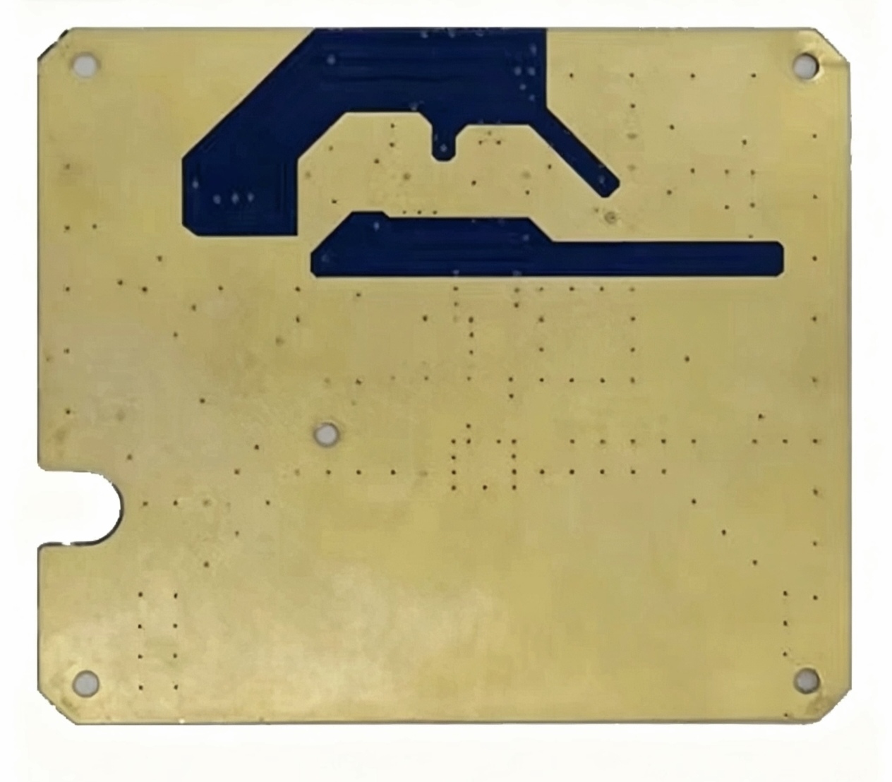
Transient current produces interference mainly through the inductance of the trace, and inductance falls as width rises and length falls. Nets that carry large transients, such as clock lines and bus drivers, should therefore be as short as the layout allows and wider than the average signal. As a rule of thumb, discrete circuits are well served by traces around 1.5 mm, while integrated circuit designs typically work between 0.2 mm and 1.0 mm. Routing the two sides of a two-layer board orthogonally reduces coupling between them, and long parallel runs on the same layer should be avoided. Where parallel runs are unavoidable, the spacing rules in this article on the 3W rule for crosstalk are the simplest way to keep coupling predictable.
Grounding: One Point or Many
Grounding is the single most effective interference control available, and it is also the one most often handled by habit. The choice between single-point and multi-point grounding follows frequency. Below roughly 1 MHz the impedance of the wiring dominates and circulating ground currents are the main problem, so all returns should meet at one point. Above about 10 MHz the ground impedance itself becomes significant, and the return should be made as short as possible at each device. Between 1 MHz and 10 MHz a single-point scheme still works provided the longest ground conductor stays under one twentieth of a wavelength at the highest frequency of interest. The broader layout consequences are covered in this article on ground routing and power trace planning.
Separating Digital and Analog Returns
When a board carries both fast logic and linear circuitry, the two sections should be physically separated and their returns should not be mixed. Each group connects to the supply return at its own point, and the analog section should have as much ground area as the layout can give it. Ground conductors also need to be wide. A thin return rises in potential as current changes, which shifts logic thresholds and degrades noise margin; a practical minimum for a main ground conductor is 3 mm, sized to carry the board current rather than to fit the available space. On a mostly digital board, closing the ground structure into a loop reduces the potential difference between distant points and improves noise immunity noticeably.
Reviewing the Rules as a Set
Individual rules are easy to satisfy in isolation and easy to lose when a layout is squeezed. The useful discipline is to review the board once with the rules in front of you, checking placement groups, decoupling loops, thermal ordering, trace widths and the return structure together. At gopcb that review is a standard step before a design is released, because the cost of a revision is far higher than the cost of an hour spent reading the layout against the checklist.
FAQ
How do I choose between single-point and multi-point grounding? Use single-point below about 1 MHz, multi-point above about 10 MHz, and in between use single-point only if the longest ground conductor is shorter than one twentieth of a wavelength.
Is one decoupling capacitor per chip still necessary? It is the safest default. Where space forces a compromise, one 1 uF to 10 uF capacitor shared by four to ten devices is acceptable if each device still has a short return path.
How much board spacing is needed for convection cooling? A gap of at least 20 mm between parallel boards is a reasonable starting point, with hot devices placed downstream in the airflow and away from temperature-sensitive parts.