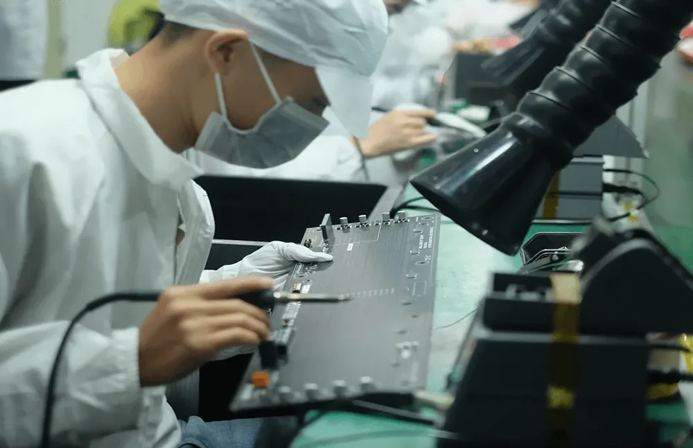
Automotive Chip PCB Layout: Placement, Power Decoupling, and EMC Guidelines
Automotive control modules are built around a system-on-chip or a multi-die module that combines a processor, memory interfaces, and a set of high-speed serial links in a single package. The layout around that package decides whether the module survives the temperature swings, vibration, and electrical noise of a vehicle, and it decides how much margin the EMC test house will find. This article covers the layout decisions that matter most for automotive chip PCB layout, from initial floorplanning through verification.
The governing constraint is different from consumer electronics. A module is expected to operate for ten to twelve years, across a temperature range that can span from minus forty to plus one hundred and twenty-five degrees at the board surface, and it has to keep working while sharing a wiring harness with motors, relays, and ignition systems. Layout choices that seem cosmetic on a bench prototype become reliability and compliance issues in the vehicle.
Component Placement Around the Package
Start with the central device and treat everything else as a satellite. The processor or module should sit where its high-speed interfaces can reach the connectors with the shortest possible routing, and where the power stage can be placed close enough that the supply impedance stays low. Memory devices paired with the processor belong on the same side of the board whenever the interface speed allows it, because vias add both inductance and reflections to a parallel bus.
Establish a clean separation between functional blocks during floorplanning rather than during routing. The power stage, the digital core, the sensor interface, and the communication transceiver each get a region, and the regions get boundaries that routing is not allowed to cross except at defined points. Layout that mixes these blocks freely produces a board that functions on the bench and fails radiated emissions testing, which is the most expensive kind of rework because it usually requires a new fabrication cycle.
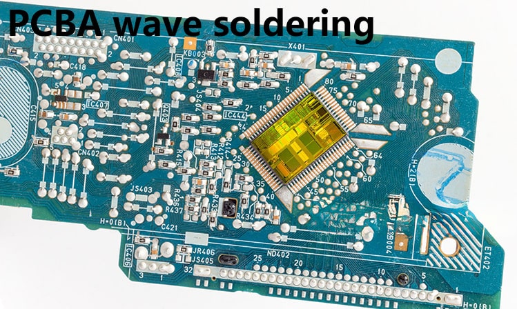
Placement order also determines how much rework the routing will need. Fixing the connectors, the crystals, and the regulator before the passive components are scattered generally produces a shorter and cleaner routing solution than placing by schematic order.
Heat-Generating Parts and Thermal Separation
Power transistors, current-sense resistors, and any switching stage dissipate enough heat to shift the local reference of a precision analog circuit. Place these parts at the board edge or in a region with an obvious thermal path to the enclosure, and keep a defined distance from the central device so the package does not sit in their thermal plume.
Where the module dissipates significant power itself, the layout should provide a deliberate vertical path: thermal vias under the exposed pad, connected to internal copper and to a spreader on the opposite side. The dimension that limits how much copper can be plated into those vias is the board thickness, so a thin core with a stiffener usually outperforms a thick board with the same drill size.
Sensitive Components: Clocks, Crystals, and Analog Front Ends
Crystal oscillators and clock generators belong as close to the device pins they serve as the layout allows, with a solid, undisturbed ground reference underneath and no routing passing beneath the package. Keep them away from switching nodes, from the board edge, and from any mechanical feature that can transfer stress to the package during thermal cycling.
The same logic applies to analog sensor inputs and reference circuits. Separate them from digital switching activity by distance first and by a grounded guard structure second, and avoid running a sensitive trace parallel to a high-current trace for any appreciable length. The coupling mechanisms and the spacing rules that limit them are described in the 3W crosstalk rule.
Power Decoupling on Every Supply Pin
Power decoupling is not a single capacitor placed near the device; it is a distributed network. Every supply pin of the module needs a ceramic capacitor placed within a few millimeters, with its ground via adjacent to the pin and its loop area as small as the layout permits. Where the device has multiple rails, each rail is decoupled independently, because a shared capacitor cannot respond to the transient on a different rail.
Value selection follows the frequency band rather than the schematic convention. Bulk capacitance on the regulator output handles load steps in the tens of microseconds, ceramic parts close to the package handle the sub-microsecond band, and a small number of very low inductance parts handle the edge rates of the internal switching. Bulk parts placed far from the load still help at low frequency, but they cannot compensate for a missing high-frequency capacitor at the pin.
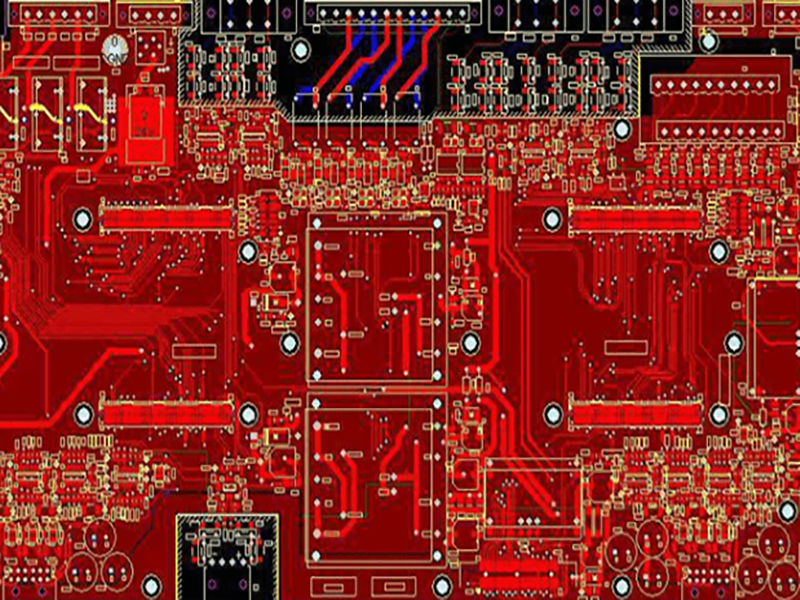
Trace geometry matters as much as capacitance value. A capacitor connected through a long, thin trace is dominated by that trace inductance at high frequency, which is why the shortest possible connection to a plane pair is always the right choice. Detailed guidance on pad sizing and land patterns, including thermal relief design for high-current joints, is available in PCB pad design standards.
Power Rail Routing and Segmentation
Power traces on an automotive board must be sized for the current they carry at the maximum ambient temperature, not at room temperature, because copper resistivity rises with heat and the trace that is adequate on the bench becomes a fuse in the vehicle. Remember derating: a trace calculated to a specific temperature rise at 25 degrees needs more width at 105 degrees for the same current.
Segment the rails by function. Digital core, memory, input-output, and analog supplies should be separated so that noise on one rail does not reach another through a shared impedance. Connect the segments where the regulator or a filter element already provides isolation, not with a random copper bridge, and place vias in groups rather than singly so that the plane connection itself has low impedance. Transmission of high-current and ground return paths is covered in ground routing and power trace planning.
Signal Integrity in the Routing Rules
Keep high-speed routing short, direct, and matched. Clock lines and serial interfaces should avoid stubs, sharp corners, and unnecessary layer changes; each layer transition should be accompanied by a return via within a fraction of a millimeter so the return current has a defined path. Where a controlled impedance is specified, the trace geometry has to be calculated against the actual stackup, including the prepreg thickness and the copper thickness after plating.
Isolate signal classes during routing. Digital switching signals, clock lines, and analog inputs should not share parallel corridors, and high-speed differential pairs should keep constant spacing and symmetry from the driver to the receiver. Any deviation from the intended geometry creates a mode conversion that shows up as common-mode radiation, which is exactly what the EMC test will find.
Ground Planes and Electromagnetic Compatibility
A continuous ground plane is the single most effective tool for electromagnetic compatibility on an automotive board. Split ground planes create return-current discontinuities and generally create more problems than they solve; where analog and digital grounds must be distinguished, define the boundary in the schematic and connect the regions at one controlled point rather than allowing accidental bridges.
Filtering at the interfaces closes the remaining paths. Place capacitors, inductors, or ferrite beads at the connector entry of each power and signal line, before the routing reaches sensitive circuitry, so that noise picked up by the harness is attenuated at the boundary. Keep the filtering components grounded to the same reference as the device they protect. Group high-frequency and high-power circuitry together and away from low-level circuitry, and keep return loops small everywhere, because loop area is what radiates.
Design for Manufacturability and Test
Design for manufacturability limits the number of surprises between prototype and series production. Pads must match the package land pattern with appropriate solder joint geometry, and fine-pitch or ball-grid packages need special attention to aperture size, spacing, and surface finish. Thermal relief on large copper areas keeps solderable joints from becoming heat sinks that never reach reflow temperature.
Test access is equally important in automotive work, because field returns have to be diagnosed and repaired. Provide test points on every supply rail, on the ground reference, and on the critical signal nodes, with enough spacing for a probe and enough mechanical access to reach the device. Design in enough clearance around parts that are likely to be replaced, and keep the silkscreen marking legible after conformal coating, since coating hides the copper features that a technician would otherwise identify visually.
Verification Before Release
Simulation should cover the interfaces that cannot be probed easily: timing margin and eye diagrams on the high-speed links, reflection and crosstalk on the parallel buses, and the impedance curve of the power delivery network across frequency. Corner-case analysis at the temperature extremes is more valuable than a nominal simulation, because the automotive operating window is wide enough that a design with no margin at 25 degrees will fail at 105.
On hardware, measure emissions and immunity early using a pre-compliance scan rather than waiting for the formal test house appointment. Pre-compliance identifies the offending interface while the board can still be modified, and a scan of the final prototype confirms that no change introduced a new resonance.
FAQ
Should the automotive module be placed on the top or bottom side of the board? Place it on the side that gives the shortest connection to the connectors and the most direct thermal path to the enclosure. For most modules this is the top side, which also keeps the assembly order simple and allows the bottom side to be dedicated to a stiffener or a heat spreader.
How many decoupling capacitors does an automotive SoC really need? Plan one ceramic part per supply pin for the high-frequency band, plus bulk capacitance on each regulator output sized by the load step. Reducing the count below one per pin should be justified by the plane impedance simulation, not by board area, because missing high-frequency decoupling rarely shows up until the module is installed in the vehicle.
Is a four-layer stackup enough for an automotive control board? For a module with high-speed serial interfaces, four layers are usually the practical minimum but often insufficient, because two inner layers must serve both power and ground while remaining continuous under the high-speed routing. Six layers give a clean ground plane, a clean power plane, and two signal layers, which is a more comfortable starting point for a design that must pass EMC on the first attempt.