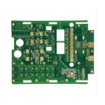
AI Computing Board Design: Five High-Performance Layout Challenges
Accelerator cards and AI server compute trays have become the most demanding boards in mainstream electronics. A single package can present several hundred high-speed differential pairs, draw well over five hundred watts, and switch between idle and full load in microseconds. Once those numbers appear in the requirements document, the board stops being a wiring platform and becomes a performance-limiting subsystem. Good AI computing board design is therefore an exercise in managing five coupled problems at once rather than a matter of completing a netlist.
The order in which those problems appear is predictable: signal integrity first, then power delivery, then heat, then routing density, and finally the verification effort that ties them together. Each one constrains the others, and each has a set of practical rules that can be applied before simulation results are available.
Challenge One: Signal Integrity Above 100 Gbps
SerDes lanes on current accelerator packages run above 100 Gbps per lane, with 112 Gbps PAM4 links now commonplace and 224 Gbps in sampling. At those rates the printed trace behaves as a lossy transmission line: insertion loss, return loss, and crosstalk all scale with frequency, and the dielectric loss tangent starts to dominate over copper roughness.
Three decisions carry most of the result. The stackup must place every high-speed layer adjacent to a solid reference plane so that the return current has a defined path with no plane splits underneath. The channel must be short enough that the loss budget closes without aggressive equalization, which usually means placing the retimer, switch, or connector on the correct side of the package rather than optimizing the routing after placement is frozen. Finally, differential pairs must be matched in length and kept at constant spacing through the entire channel, including the escape region, since a discontinuity near the ball field cannot be corrected downstream. Practical matching limits and tuning geometries are discussed in serpentine routing and length matching.
Challenge Two: Power Integrity Under Fast Load Steps
Power delivery on an AI board is harder than on a general-purpose board because the load is both large and impulsive. When an accelerator moves from an idle state to full utilization, the current step can reach hundreds of amperes in a few hundred nanoseconds, and the resulting voltage droop on the core rail has to stay inside a window measured in tens of millivolts.
Delivering that power integrity performance requires a low-impedance path from the voltage regulator to the die across the whole frequency range of interest. The regulator handles the low-frequency band, bulk capacitance covers the mid band, and ceramic capacitance close to the load covers the high band. What makes or breaks the design is the impedance of the planes and vias in between: a narrow neck in the plane, a row of anti-pads, or a via field with too few return vias can add more impedance than the capacitors remove. Splitting rails and referencing them properly is covered in power plane splitting rules.
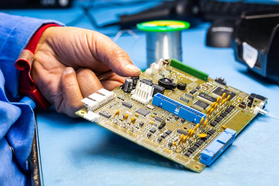
Simulation should be run on the plane model, not on the netlist alone, because the plane geometry is what determines whether the target impedance curve is actually met between 1 MHz and 100 MHz.
Challenge Three: A Decoupling Capacitor Strategy That Scales
Simply adding capacitance does not fix a droop problem. Each decoupling capacitor contributes useful charge only up to its self-resonant frequency, so the capacitor value and package size have to be chosen against the frequency band they are expected to cover. A 100 nF part in an 0402 body stops behaving capacitively well below the range where package inductance dominates.
Three layers of decoupling work well in practice. Bulk electrolytic or polymer capacitors near the regulator handle the slow transient. Small ceramic parts scattered under and around the package handle the mid band. Where the highest frequencies matter, capacitance embedded in the laminate places charge within a fraction of a millimeter of the die and removes the via inductance from the loop entirely. The layout rule that matters most is loop area: the capacitor ground via must sit directly beside its power via, and both must connect to planes that are continuous under the device.
Challenge Four: Removing Heat From a Power-Dense Package
Power density at the package level now exceeds what lateral spreading through the laminate can handle. Heat has to be pulled downward through the board as well as upward into the heat sink, and the board has to be designed for that path from the first placement iteration.
The standard technique is a dense array of thermal via structures under the die shadow, connected to internal copper planes and terminated in a spreader or stiffener on the secondary side. Aspect ratio governs how much copper the fabricator can plate into those holes, so thermal vias also need to be considered during stackup selection rather than added afterwards. A 0.3 mm hole in a 3 mm board is a very different thermal element from the same hole in a 1.6 mm board. Where lateral spreading is still required, embedded copper coins or vapor chambers reduce the peak junction temperature significantly compared with a plain laminate path.
<img src="https://www.gopcba.com/wp-content/uploads/2026/08/high_density_pcb.jpg" alt="Thermal via array under an AI accelerator package” />
Thermal design and power delivery share the same copper, so any change to the plane structure late in the project should be re-checked against both the impedance curve and the junction temperature.
Challenge Five: High-Density Interconnect and BGA Escape
Packages with several thousand balls cannot be escaped on a conventional multilayer stack without consuming an unreasonable number of layers. HDI PCB construction answers this by adding microvia layers that allow signals to change reference planes close to the ball field, freeing inner layers for power and long-haul routing. Sequential lamination, filled microvias, and via-in-pad structures make the escape possible with two or three thin dielectric layers instead of six thick ones.
The constraint to respect is structural reliability. Stacked microvias concentrate mechanical stress, and unfilled or poorly filled vias can crack at the barrel during thermal cycling. Any structure deeper than two stacked levels should be qualified with cross-sections after thermal stress. Escape design rules, fan-out patterns, and the trade-off between dog-bone and via-in-pad escapes are covered in escape routing and fan-out rules.
Bringing the Five Problems Together
Modern AI board layout is not a sequential flow. Thermal maps feed the power integrity model, the power model feeds the placement of decoupling, the placement of decoupling determines where signal layers can run, and the signal layers determine the stackup that the thermal path must pass through. Teams that run these analyses in sequence usually discover the conflict after the stackup is released.
Two practices shorten the loop. First, build a single model that carries the power loss map into the thermal solver, so that the heat sources are the actual simulated losses rather than an assumed uniform value. Second, hold a joint review that includes the hardware architect, the layout engineer, and the thermal engineer before placement is fixed, so that device selection and floorplanning are decided against all three sets of constraints at the same time.
Where the Technology Is Heading
Chiplet integration is already changing the board’s job description. When several dies are interconnected inside the package through an interposer or a bridge, the board becomes responsible for connecting packages rather than individual dies, which concentrates bandwidth into a smaller number of very wide, very fast interfaces. Co-packaged optics pushes further by moving the optical engine next to the switch or compute die, so the board must carry high-speed electrical signals to a photonic interface and manage the thermal load of the optical assembly at the same time.
Both trends raise the same requirement: the board has to be designed as an electrical, thermal, and mechanical system with tolerances tight enough that package-level decisions remain valid. Boards that treat the package as a black box with a pin list will not be able to meet the next generation of interfaces.
FAQ
How much insertion loss is acceptable on a 112 Gbps PAM4 channel? Most implementations target roughly 20 to 28 dB at Nyquist including the package and connector, with the remainder handled by equalization in the transmitter and receiver. Anything above that range should be resolved by shortening the channel or changing the laminate rather than by relying on stronger equalization.
Can I skip embedded capacitance and still meet the target impedance? Often yes, provided the ceramic capacitors are placed with minimal via loop inductance and the planes are continuous under the package. Embedded capacitance becomes necessary when the required impedance must be held above roughly 100 MHz across a large area, where discrete parts simply cannot be placed close enough. thermal management also improves because the thin dielectric reduces the vertical thermal resistance.
What is the most common cause of a failed AI board bring-up? In practice it is a power integrity problem rather than a signal integrity problem, and most often a plane or via bottleneck that the pre-layout impedance sweep did not model. Measuring the droop at the package pins under a real load step, then comparing it with the simulated curve, identifies the discrepancy quickly.