PCB Design and Prototyping: Optimizing the Development Flow
Prototyping is where a design stops being a drawing and starts producing data. The schedule risk in a hardware project is rarely in the schematic; it sits in the two or three weeks between finishing the layout and holding a working board, and most of that time is lost to rework rather than to the fabrication queue itself. Treating PCB design and prototyping as one continuous flow, with the layout constrained by what the prototype stage needs, removes a large part of that loss and shortens the loop between a measurement and the change it justifies.
Where Prototyping Fits in the Schedule
The prototype has a specific purpose: to find the errors that analysis cannot. If the layout is released before the questions that the prototype will answer are known, the first build has to answer everything at once, and a single failure can hide several causes. It helps to write down, before releasing the design, which nets will be measured, which rails will be loaded, and which thermal and mechanical limits will be checked. That list determines what test points and copper the layout must include, and it is much cheaper to add them before the Gerber data is generated.
Design Rules That Keep the Prototype Buildable
The layout should be drawn to the capability of the intended fabricator from the first day, not corrected afterward. Minimum trace and space, via drill and annular ring, solder mask expansion, and the smallest silkscreen line the process can print are all fixed numbers that the designer should confirm rather than assume. Components with fine pitch need enough room for the assembly process, including the courtyard and the stencil aperture. These constraints are collected in this article on PCB design guidelines that keep a board manufacturable, and applying them at layout time is what prevents a board that is electrically correct from being physically unbuildable.

Signal Integrity Analysis Before the Layout Is Frozen
Signal integrity analysis is most useful while changes are still cheap. Impedance targets for single-ended and differential nets should be derived from the stackup, and the resulting trace geometry should be checked before routing rather than after. Length matching rules for parallel buses, the position of the longest stub, and the reference plane under each fast net are all items that a pre-layout analysis can confirm in an hour and that a post-layout discovery can cost a revision. The geometry that governs those calculations is described in this article on microstrip and stripline routing.
Generating and Checking Fabrication Data
The fabrication package should be generated from a frozen design database, not from a working copy that has been edited for the last-minute change. It usually contains copper and solder mask layers, drill data, the layer stackup with material and finished thickness, a bill of materials, and an assembly drawing with polarity and orientation marked. A simple visual check of each Gerber layer against the design, and a netlist comparison, catches the majority of errors that reach fabricators.

Choosing a Fabricator and Comparing Quotes
Fabricator capability should be matched to the board rather than to the lowest price. Two houses may both quote the same board, but one may achieve the smallest vias with a different process, and the difference shows up in yield rather than in the quotation. For a first prototype it is usually worth accepting a slightly higher price to get engineering support, because questions about the stackup or the impedance tolerance are answered faster and more accurately. Standard panel sizes and common materials reduce cost more than aggressive feature sizes increase it.
Quality Control on the Prototype Batch
Quality control on a prototype is not the same as quality control in production. The goal is not to measure yield but to prove that the board can be inspected at all. Visual inspection, electrical test of every net, and a check of solder joint formation on the fine-pitch parts will show whether the design allows adequate process windows. If a joint cannot be inspected on the prototype, it cannot be inspected in production either, and the layout should be changed while the volume is still small. The characteristics worth checking are described in this article on PCB design quality characteristics.
Reading Test Results and Iterating
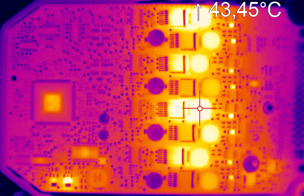
Each design iteration should start from a measurement rather than an impression. A rail that droops under load points to the distribution network; a signal with visible overshoot points to a termination or a reference plane problem; a device that runs hot points to thermal spreading. Recording which change produced which result builds an internal record that makes the next project faster. A revision should be limited to the changes that the measurements justify, because a revision that also fixes unrelated details cannot be evaluated.
Validating Before Volume Production
Before committing to volume, a small batch produced on the same process and the same equipment as production confirms that the design is repeatable. Panel utilization, tooling, and the assembly sequence all behave differently at volume, and a problem found here costs far less than one found after tooling is committed. Sign-off should include the fabricated stackup, the measured impedance, the electrical test result and the thermal data, so that the production file set is supported by evidence rather than by assumption. If any of those measurements is missing, the gap should be closed with a deliberate test rather than with a note, because the production process will reproduce whatever the design actually does and not what the documentation says it should do.
Prototype Fabrication Options
Prototype fabrication is available in several forms, and choosing between them changes both the cost and the value of the result. A quick-turn service with a standard stackup is the fastest way to confirm that the circuit works, but it usually fixes the material and the layer construction, so impedance and thermal behaviour may differ from the production board. Building the prototype on the intended production stackup costs more and takes longer, yet it is the only way to validate controlled-impedance routing and thermal spreading under realistic conditions. A middle path is common: use a fast, inexpensive board for the first functional check, then re-fabricate the same design on the production stackup once the circuit is known to work. Whichever route is chosen, the artwork and the drill data should be identical, so that the second build answers a narrower set of questions. Recording which stackup was used for each build prevents a confusing comparison later, and it keeps the prototype fabrication record aligned with the final production release.
FAQ
How long should a prototype cycle take? Bare board fabrication is typically a few days and assembly a few more, so most of a two-week cycle is layout review and test preparation rather than manufacturing.
Should the prototype be built with the production stackup? Yes. Using a different material or layer construction for the prototype invalidates the impedance and thermal results that the prototype is meant to prove.
What is the most common cause of a delayed prototype? Incomplete fabrication data. Missing drill or stackup information generates an engineering query that can add days before the board is even scheduled.