AI Smartphone PCB Design: Compute Density, Signals and Heat
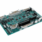
Smartphones stopped being simply “smart” once they began running inference locally. Adding a neural processing unit to an application processor changes far more than the bill of materials: it turns the main board into a compute platform where every square millimetre has to justify itself. AI smartphone PCB design is the discipline that makes that trade-off work, balancing compute density, signal integrity, power delivery and heat inside a chassis that cannot grow.
Why On-Device AI Changes the Board
The pressure arrives from three directions at once. Compute density rises because the application processor, the neural engine and often a dedicated accelerator now share one footprint. Data volume rises because image sensors, depth sensors, high refresh displays and 5G or 6G radios all push samples into memory in real time. Meanwhile the enclosure still has to hold a battery, a camera stack and an antenna farm. The result is a board where routing channels, copper area and thermal paths are contested resources.
Engineers who treat the main board as a passive carrier of components run into trouble quickly. At these data rates the interconnect is part of the circuit. A few hundred micrometres of extra trace length, or a reference plane that is not continuous under a differential pair, can turn a clean link into a marginal one, and marginal links fail intermittently as temperature changes. The design therefore has to start from a stackup and a floorplan decision rather than from a finished net list.
Thermal Management Begins at the Floorplan
Heat is the first constraint that shows up, because sustained inference keeps the processor at high power for seconds rather than milliseconds. Vapour chambers and graphite sheets spread heat, but they cannot repair a floorplan that places a three-watt processor next to a temperature-sensitive image sensor or a crystal oscillator. The practical approach is to treat the board as a heat-flow diagram: simulate the processor, memory and power stages, then place parts so hot nodes are separated from sensitive ones along the vertical axis as well as in the plane.
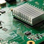
Copper becomes part of the cooling system. Thick copper on ground layers, a dense field of thermal vias beneath the processor and exposed copper under the shield can each lower junction temperature by several degrees. In stacked designs, embedded copper coins or metal slugs move heat to the rear of the board where the chassis acts as the final heatsink. Thermal management is not a late-stage correction; it is a floorplan input, and it has to be re-checked after every significant placement change.
Once heat paths and component zones are settled, the board is ready for the routing decisions that dominate electrical performance. Those decisions are made in the stackup, and the stackup is where an HDI process earns its extra cost.
Building the HDI Stackup
High-density interconnect is unavoidable when a package with more than a thousand balls sits a few millimetres from LPDDR memory. Any-layer microvia construction, in which laser-drilled vias connect any two adjacent layers, removes the through-hole congestion that would otherwise block escape routing from the processor. The available blind and buried via stack options keep plane layers intact under the densest areas, while via-in-pad with copper filling lets escapes begin directly at the ball instead of being offset into a dogbone.
Every one of those choices has a manufacturing boundary. Microvia diameters below 0.1 mm, stacked microvias and filled via-in-pad all raise cost and yield risk, so they should be reserved for the nets that genuinely need them. A useful rule is to define the HDI stackup as a set of zones: the finest geometry over the processor and memory footprint, a mid-range geometry for power and clock distribution, and conventional through-via geometry everywhere else.
Signal Integrity at Memory and SerDes Rates
LPDDR5X links and PCIe 4.0 or 5.0 lanes leave very little timing margin. Controlled differential impedance, typically 85 to 100 ohm, has to be held from the package ball to the far end, with an unbroken reference plane along the whole path. A plane split forces return current to detour, which adds inductance and radiates. Where a split is genuinely unavoidable, stitching capacitors placed within a millimetre of the crossing keep the return loop short.
Length matching matters, but so does the shape of the matching. Serpentine tuning should keep coupled sections short and use a pitch of at least three times the trace width so the tuning does not create new crosstalk between adjacent turns. In high-frequency trace and data bus routing, keeping the layer transition count low is usually worth more than shaving a fraction of a millimetre from the route. Every via adds stub and discontinuity, and back-drilling or blind vias remove the stub on the fastest lanes.
Power Delivery Network and Decoupling
A processor that idles at a few hundred milliwatts and then draws amps within microseconds places extreme demands on the power delivery network. The impedance of the PDN has to stay under a target curve from DC to several hundred megahertz. That is achieved in layers: bulk capacitors close to the regulator, mid-frequency ceramics distributed around the processor, and low-inductance decoupling as near to the ball grid as the rules allow, ideally on the opposite side of the board directly under the die.
Plane pairs do most of the heavy lifting. A thin dielectric between a power plane and its adjacent ground plane provides a low-impedance, high-frequency reservoir that no discrete capacitor can match. The usual power plane splitting rules apply here: arrange the splits so a high-speed signal never crosses from one rail region to another on the same layer, because a continuous return path is worth more than a marginally shorter power connection.
Packaging, Sensors and Front-End Integration
At the top of the range, package-level integration moves the boundary of the board design. System-in-package assemblies place the processor, memory and sometimes a wide high-bandwidth memory stack on a silicon interposer, so the board no longer routes those nets at all; it supplies power and a much smaller set of high-speed interfaces. This makes the package substrate the critical medium and shifts the board task toward managing warpage, coefficient of thermal expansion mismatch and cross-scale signal transfer.
Sensor integration runs in the opposite direction. Camera, time-of-flight, microphone array and radar front ends benefit from short analog paths to a local pre-processing stage, which then links to the processor over a single high-speed interface. Grouping those analog front ends, giving them a quiet reference and keeping switching regulators out of that zone prevents the noise floor from rising under load. This is ordinary mixed-signal discipline applied inside a very small area.
None of these decisions can be validated by inspection alone. Simulation, from thermal maps to electromagnetic field solving on the fastest nets, is what turns an aggressive layout into a manufacturable one. The flow and the physical board have to be developed together from the first week of the project.
Constraint-Driven Flow and Verification
Constraint-driven layout is the practical answer. Impedance, length, spacing and plane rules are captured as constraints in the layout database, so the router is guided rather than corrected afterwards. Electromagnetic simulation of critical nets and a full-board power integrity sweep catch problems a design rule check cannot see. Machine-learning-assisted tools are beginning to search parameter spaces such as trace width, via position and layer assignment for solutions that satisfy electrical, thermal and mechanical limits at once, but the engineer still owns the constraints.
Prototype builds remain the final test. Time-domain reflectometry on controlled-impedance nets, thermal imaging under sustained inference load, and conducted and radiated emissions scans all show whether the model matched reality. Because the mechanical envelope is fixed, every fix has to fit inside the same footprint; that is why rework margin, spare vias and a spare routing layer are worth planning into the first revision.
What Comes Next
Two directions are already visible. Optical interconnect, today confined to data centres, will move down to the handset as data rates push copper past its practical limit, and that requires the board to host optical waveguides and mixed electrical-optical signal paths. Structural integration continues in parallel, with antennas, thermal hardware and even battery elements becoming part of the board frame instead of separate parts.
For engineers, the practical conclusion is that the main board of an AI handset is a system-level design problem. Compute, power, heat and signal integrity are coupled, and each has to be solved in the same small volume without breaking the others.
FAQ
How many layers does an AI smartphone main board need? Typical designs run 10 to 14 layers with any-layer microvias over the processor and memory footprint. The exact count is set by the number of power rails, the escape density under the package and the need for solid reference planes under the fastest interfaces.
Is via-in-pad always required under the processor? No. Filled via-in-pad is used where escape routing is blocked and the ball pitch is too fine for a dogbone. In less dense areas, standard microvias keep cost lower without hurting electrical performance.
How much layout work happens before the schematic is frozen? Floorplanning, stackup definition and thermal zoning normally start as soon as pin-out and package data are known. Waiting for a frozen net list wastes weeks, because placement constraints often feed back into schematic and package decisions.