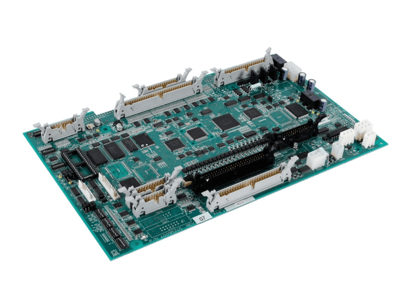
MCU Control Board Layout: Decoupling and Grounding Rules
A microcontroller control board for a small appliance looks simple: an MCU, a few driver stages, a display, some buttons and a power supply. In practice it is one of the harder boards to get right, because the same board carries switching currents, low-level analog measurements and a clock oscillator within a few square centimetres. MCU control board layout decides whether the product passes its own noise tests, and the rules for getting there are well established.
Placement Rules Around the Microcontroller
Start by separating noisy from sensitive. Clock generators, crystals, switching regulators, relay drivers and motor drivers all generate interference; the MCU logic block, memory and analog measurement circuits are the victims. Place noisy parts at the far edge of the sensitive group, and if a switching stage is large enough to justify a separate board, keep it separate and connect through a filtered interface. Components that belong to the same function should sit close together so loop areas stay small.
The MCU itself is normally placed centrally, but the more useful rule is that its support components follow it. Clock circuit, reset circuit, decoupling and programming header all belong within a few millimetres of the pins they serve. Anything that forces a long trace to one of those pins will collect noise and reduce the timing margin.
Decoupling Capacitor Placement and Value
Every supply pin needs a local decoupling capacitor, typically 100 nF for digital pins, with a larger bulk capacitor shared by the rail. The capacitor is only useful if the loop from its pad through the pin and back to ground is short, so it should be placed on the same side of the board as the MCU where possible, with the via to the ground plane adjacent to the capacitor pad rather than at the far end of a trace.
Trace inductance is the enemy here. A decoupling capacitor connected by two long thin traces behaves as an inductor at exactly the frequencies where it is supposed to work. Keeping the capacitor within a couple of millimetres of the pin, using short wide connections and placing the ground via first are the practical rules. On boards with a ground plane, the plane itself provides the return path, and the capacitor only needs to reach the nearest via.

The supply is only half of the noise problem. The other half is the reference, and on a mixed-signal control board the ground strategy determines measurement accuracy.
Separating Analog and Digital Ground
Analog and digital returns carry different current waveforms and should not share a conductor. Route the analog ground as its own net, connect it to the analog supply return, and keep digital switching currents out of it. The analog ground pour should be generous, with a wide connection to the ground pin of the analog supply, and analog input and output signals are best isolated from the MCU through an optocoupler or a digital isolator where the design allows it.
The two grounds still have to meet somewhere, because signals cross between the domains. Join them at a single point, ideally underneath the converter or amplifier that bridges the domains, so the return current follows a defined path instead of wandering through the analog area. These are the standard mixed-signal PCB design guidelines, and they are easier to apply on a small control board than on a large one.
Single-Point or Multi-Point Grounding by Frequency
Grounding topology follows frequency. Below about 1 MHz, the impedance of the ground connection is dominated by resistance and by circulating currents, so a single-point ground that avoids loops is the better choice. Above roughly 10 MHz, trace and plane inductance dominates, and a multi-point ground that provides many parallel return paths has lower impedance than any single-point arrangement.
Most control boards span both ranges, which is why the practical answer is a solid ground plane with the analog section referenced to it at one defined location. The plane provides the low-inductance return path at high frequency, while the single tie point keeps low-frequency circulating currents out of the analog region.
Ground Trace Width and Return Paths
Where a plane is not available, ground traces have to be sized for current. A ground trace that is too narrow develops a voltage drop that moves with load current, which shifts logic thresholds and corrupts analog readings. A practical minimum for a main ground path is 2 to 3 mm in width on a board of this class, with component ground pins connected through traces of at least 1.5 mm.
Return paths should be planned as carefully as the signal paths, especially on two-layer boards. A signal trace that runs across a split in the ground pour forces its return current to take a long detour, which increases loop area and radiates. Keeping a continuous return path under every sensitive signal is more effective than adding shielding later.
Clocking and interfaces are the remaining sources of trouble, and both are predictable if the layout follows a few physical rules.
Crystal Oscillator and Clock Routing
The crystal oscillator and its load capacitors belong immediately next to the MCU clock pins, with the shortest possible traces and a local ground island underneath. No other signal should run through that area, and the ground island should be connected to the main ground plane by several vias. Guarding the clock traces with ground on both sides, or routing them on an inner layer between ground planes, reduces coupling to the rest of the board.
Clock traces should be kept short and routed away from connector pins and analog inputs. Where a clock must travel across the board, treat it as a controlled-impedance line and keep the reference plane continuous. Spacing clock and other periodic signals at least three times their trace width apart, the familiar 3W crosstalk rule, is a reasonable starting point for reducing coupling.
Isolation and Interface Protection
Appliance control boards connect to the outside world through buttons, sensors, relays and communication ports, and those connections bring in transients. Isolation through optocouplers, or a combination of series resistance, clamping diodes and a transient suppressor, keeps the disturbance away from the MCU. The isolation barrier should have a clear keep-out with no copper crossing it except the intended coupling element.
Driver circuits for relays and motors deserve the same care. The freewheeling diode must sit directly across the coil with a short loop, and the driver return should not share copper with the MCU ground. A ground-stitched layout for the power stage keeps switching currents contained, and the ground and power routing plan should be drawn before signal routing begins.
FAQ
Do I need a four-layer board for an MCU control board? Not always. Two layers can work if a solid ground pour is maintained on the bottom layer with few interruptions. Above roughly 20 MHz, or with analog measurements below one millivolt, four layers with dedicated ground and power planes are easier to make reliable.
How many decoupling capacitors per supply pin? One 100 nF capacitor per supply pin is the standard, plus one bulk capacitor of 4.7 to 22 uF for the whole rail. Additional values add little unless the plane structure is poor.
Can the analog and digital grounds be connected directly? They must be connected, but at one point. Connecting them everywhere defeats the separation and lets digital switching currents flow through the analog reference.