AI Mainboard PCB Design and Fabrication: Materials, Process and Test
Accelerator cards, edge inference appliances and AI servers all share the same physical problem: a very large processor package that has to be fed with clean power, kept cool and connected to memory and peripherals at rates that leave almost no margin. AI mainboard PCB design and fabrication is where those requirements meet the limits of laminate processing, and the two halves of the job cannot be separated. A design that ignores what the fabrication house can hold will not survive first article inspection, and a build plan that ignores stackup impedance will not pass validation.
What Makes an AI Mainboard Different
The obvious difference is pin count. Accelerator packages commonly present two thousand or more balls on a pitch of 0.8 mm or finer, which means the escape routing alone consumes several routing layers before a single functional net is connected. The second difference is channel loss. Serial links between processors, switches and memory run at 25 to 56 Gbps per lane, so the laminate becomes a transmission medium rather than a mechanical support. The third is current: a board that delivers several hundred watts at 0.8 V has to move hundreds of amps through the power planes with ripple measured in millivolts.
Those three pressures interact. Adding layers to solve escape density increases the distance between decoupling capacitors and the die. Choosing a lower-loss laminate to protect the high-speed channels changes the thermal conductivity and the drilling behaviour. Increasing copper weight for current capacity makes fine-line etching harder. Every decision has a cost somewhere else on the board, which is why the stackup review is usually the longest meeting in an AI hardware project.
Package Escape and Any-Layer HDI
Escape routing from a large ball grid array is the classic bottleneck. With a 0.8 mm pitch there is room for one or two traces between balls, and with 0.65 mm or 0.5 mm pitches the designer is forced into microvia technology. Any-layer HDI, where every layer pair can be connected by a laser-drilled microvia, removes the through-hole channels that would otherwise wall off the inner layers. Traces then drop from the ball to the first inner layer, travel a short distance and descend again, spreading out gradually instead of competing for a handful of drill positions.
Filled via-in-pad is normally the starting point for the processor footprint, because it allows the escape to leave the pad directly. Where the pitch is generous enough, dogbone fanout with a short stub is cheaper and electrically adequate. A mixed approach is common: the finest geometry over the accelerator and its memory, standard microvias in the mid-board region, and conventional through vias around connectors and power conversion. Layer counts of 16 to 24 are typical, and the advantages of multilayer construction at high speed come mostly from the solid reference planes those extra layers provide rather than from more routing.
Choosing Low-Loss Materials
At 25 Gbps and above, insertion loss is dominated by the dielectric. Laminates used for these boards are specified by dielectric constant and dissipation factor rather than by a trade name: a Dk in the range of 3.0 to 3.5 and a Df below 0.005 at 10 GHz is a reasonable target for long backplane-class channels, while shorter links inside an appliance can tolerate a mid-loss material. The choice should follow the channel budget, not the marketing data sheet, because the more expensive laminates are harder to process and often require tighter drilling and lamination windows.
Hybrid stackups are a practical compromise. The high-speed layers are built on low-loss cores and prepreg, while the power and low-speed digital layers use standard FR-4 material. The interface between the two must be planned carefully, because the coefficient of thermal expansion differs and the lamination cycle has to satisfy both. Glass style also matters: spread glass reduces the fibre-weave effect that skews differential pairs, and it is usually worth the premium on layers that carry the fastest lanes.
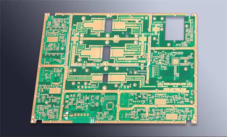
Material and geometry together define the electrical behaviour of every net, which is why impedance is specified as a manufacturing requirement rather than a layout preference. The fabrication house has to be able to reproduce it on the production panel, not just on a test coupon.
Impedance Control Through the Whole Flow
Single-ended nets on an AI mainboard usually target 50 ohm, differential pairs 85 or 100 ohm, with a tolerance of plus or minus 10 percent. Meeting that means the fabricator calculates trace width and dielectric spacing from the actual prepreg thickness after lamination, not from nominal values, and the design uses those calculated widths. Test coupons are placed on every panel and measured with time-domain reflectometry at sample frequency. If the measured impedance drifts outside the window, the whole panel is suspect.
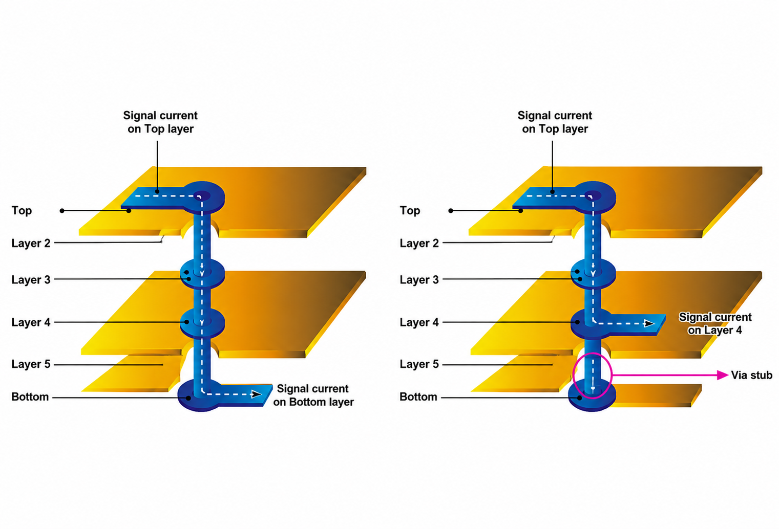
Consistency matters more than the absolute number. A channel whose impedance varies from 88 to 96 ohm along its length behaves worse than one that sits steadily at 92 ohm, because the reflections add. That is the argument for keeping the reference plane continuous, for avoiding layer transitions where possible, and for using back-drilled or blind vias on the fastest lanes so the unused barrel does not create a resonant stub.
Power Integrity and Current Capacity
Accelerator boards concentrate current. A 0.8 V rail delivering 400 A needs an effective resistance in the micro-ohm range, which means multiple plane pairs, wide copper pours and dozens of parallel vias under the regulator. Copper thickness on those layers is frequently 2 oz or more, and trace width and current calculations must account for temperature rise rather than just nominal current, because a plane that runs hot loses conductivity and ages faster.
Decoupling is layered by frequency. Bulk electrolytic or polymer capacitors handle the low-frequency envelope, mid-range ceramics cover the hundreds of kilohertz to tens of megahertz band, and low-inductance parts placed on the opposite side of the board directly beneath the die handle the fastest transients. A thin dielectric between the power and ground planes supplies the highest-frequency current locally, and EMI reduction through stackup and layout starts from the same plane pair. Simulation of the power delivery network from DC to a few hundred megahertz should be part of sign-off, not an optional extra, because a resonance in the wrong place can produce voltage droop that no amount of capacitance will fix.
Thermal Paths: Thick Copper, Vias and Inlays
Heat leaves an accelerator board through three routes: into the air, into the chassis and back down through the board. Thermal via arrays under the die, copper inlays and thick copper planes all lower the thermal resistance of that path. Where power and signal must be isolated from the heat spreading layer, a thermal-separation layout keeps the copper dedicated to conduction rather than sharing it with electrical nets. Thermal reliefs are used carefully: they keep solder joints manufacturable, but a field of reliefs in a current path adds resistance that must be accounted for.
Thermal design and electrical design should be verified together. A layout that looks acceptable at 25 degrees Celsius can fail when the regulator sits at 105 degrees Celsius and its output droops. Thermal simulation, followed by infrared imaging of a functional prototype under sustained load, is the only reliable way to confirm the model.
Turning all of this into a physical board is a process discipline. The fabricator needs a data package that describes the design intent, and the designer needs to understand which process steps set the achievable limits.
Fabrication: CAM, Lamination, Drilling, Imaging
The build starts with a design for manufacturability review in CAM. The engineer checks the drill table against the copper clearances, adjusts the artwork for etch compensation, verifies the layer-to-layer registration budget and confirms that the impedance model matches the supplied stackup. Any mismatch found here is cheap; the same mismatch found after lamination is scrap. Lamination then presses cores and prepreg with a controlled temperature and pressure profile using high glass transition temperature material, so the panel survives the thermal excursions of assembly and field operation without delaminating.
Laser drilling produces the microvias, which are then filled by copper plating to give a flat surface for the next layer. The plating must fill the via completely, without voids or dimples, or the downstream lithography will not resolve properly. Fine-line imaging uses laser direct imaging to reach 75 micrometre and finer traces, and high aspect ratio through holes must be plated with uniform copper to avoid barrels that crack during thermal cycling. Solder mask is applied with tight registration so that ball pads are not bridged, and the surface finish of choice for fine-pitch assembly is electroless nickel immersion gold, which gives a flat pad, good solderability and a long shelf life.
Test and Quality Control
Electrical test on a bare board uses flying probe or a dedicated fixture to confirm continuity and isolation on every net. Automated optical inspection checks the imaged layers for opens, shorts and nicks before lamination and after final finish. Coupon-based impedance testing, microsection analysis of via barrels and thermal cycling of test panels complete the picture. For AI hardware, in-circuit testing of the assembled board is usually extended with functional test under load, since thermal and power behaviour only appear when the board is actually doing work.
Working With the Fabrication Partner
Because so much of the design is constrained by process, the fabrication partner should be involved before the stackup is frozen. Useful questions to ask are concrete: what is the minimum microvia diameter in production, what copper weight can be imaged at the required line width, what impedance tolerance is held on a production panel, and how are stackups verified. A fabricator that can answer with numbers and samples is worth more than one that answers with a capability brochure.
FAQ
How many layers does an AI accelerator board need? Most designs fall between 16 and 24 layers. The count is driven by the escape density under the processor, the number of independent power rails, and the requirement for solid reference planes under the high-speed channels.
Can standard FR-4 be used for an AI mainboard? For the power and low-speed layers, yes. For channels above roughly 10 Gbps, a mid-loss or low-loss laminate is normally required to keep insertion loss and skew within budget.
When should the fabrication house be consulted? Before the stackup is finalised. Drill capability, copper weight limits and the achievable impedance tolerance all constrain the stackup, and changing it later forces a full re-route of the high-speed nets.