PCB Manufacturing Automation and Process Optimization
Circuit board production has become a data-driven process. Design files are converted into tooling automatically, panels are imaged with laser direct imaging instead of film, and every board carries a traceable history of the process parameters that produced it. The shift matters commercially because it moves the cost of quality from inspection after the fact to control during the process. This article describes where PCB manufacturing automation has the largest effect and how process optimization is applied on a modern line.
The production sequence itself has not changed: design data is released, fabrication builds the bare board, assembly places and solders the components, test verifies the result, and the finished assembly is packed and shipped. What has changed is how much of each step is closed-loop and how much information flows back to the earlier stages.
From Design Data to Fabrication
Production begins with a data preparation step that converts the CAD output into machine instructions. Automation here means the CAM step performs design rule verification against the fabricator’s capability profile, compensates artwork for etch factor, generates drill and routing programs, and produces the panel array. Manual intervention at this stage is where most first-article discrepancies originate, so the useful metric is not how fast the file is converted but how many conversions require a human decision.
The design rules that govern this check are the same ones the layout engineer should apply during routing, and aligning both sides on a shared rule set removes an entire class of rework. The relationship between early layout choices and production outcomes is described in how PCB layout decisions affect production.
Process Optimization in Fabrication
On the fabrication floor, process optimization concentrates on the steps with the narrowest process windows. Laser direct imaging replaces photographic film, removing the dimensional drift that comes from film stretching and improving layer-to-layer registration. Automated optical inspection after etch catches opens, shorts, and nicks before the panel receives any further value.
Plating is the other focus area. Pulse plating and automated chemistry control keep the copper grain structure consistent and distribute thickness evenly across high-aspect-ratio holes, which is what determines whether a barrel survives thermal cycling. Analysis of the plating bath is now typically continuous rather than batch-based, and the results feed an automatic dosing system, so the additive concentration does not drift between shifts.
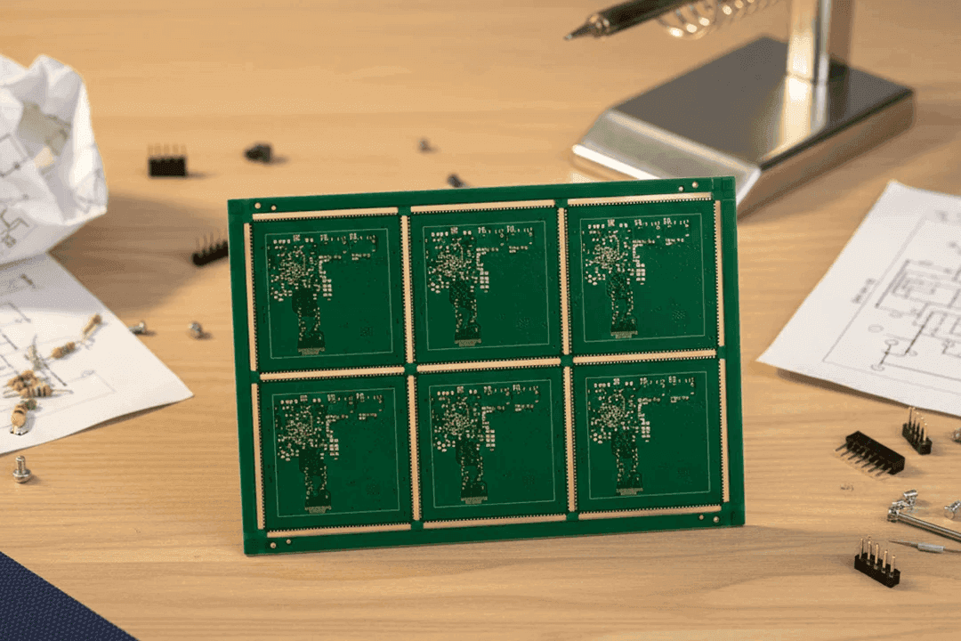
Etch compensation and registration tolerances are also adjusted per panel rather than per product family, using measured incoming material. That is how a line holds fine-line capability at scale without widening every design rule to the worst-case value.
Automation on the Assembly Line
Component placement is dominated by high-speed pick-and-place with inline paste inspection. Solder paste volume is measured after printing rather than assumed, and panels that fall outside the specification are diverted before components are placed on them, which prevents wasting parts on a board that will be scrapped. Reflow is run in a controlled atmosphere with a profiled recipe that is verified per product rather than copied from a similar assembly.
Wave soldering and selective soldering handle through-hole content, and both benefit from the same principle: control the thermal profile and the flux activity, and verify the result with inspection rather than with operator judgment. Placement accuracy and paste volume are the two variables that most often determine whether a joint forms correctly, which is the subject of SMT component shift causes.
Solder Reflow Control and Profiling
Solder reflow is a chemical process as much as a thermal one, and it has to be profiled for the actual assembly. The soak zone activates the flux and equalizes temperature across parts of different thermal mass; the ramp to peak must not exceed the component rating; and the time above liquidus must be long enough to form a proper intermetallic layer without growing it so thick that the joint becomes brittle.
Automation contributes by attaching thermocouples to a representative production panel and recording the profile for every build, rather than once at the start of the program. Where a product runs on multiple lines, each line has its own verified profile, because oven airflow and conveyor speed differ between machines even when the setpoints match.

Profile verification is also the point where a design problem becomes visible. If a large component cannot reach temperature within the allowed window, the fix belongs in the layout, for example by separating heavy parts or by providing additional thermal relief, rather than in a longer oven recipe that damages the rest of the assembly.
Inspection: Automated Optical Inspection and In-Circuit Test
Automated optical inspection compares each board against a learned reference and detects missing, misaligned, or wrongly oriented components, along with solder defects such as insufficient fillets and bridges. Modern systems program the inspection from the same CAD data used for placement, so the inspection coverage stays in step with design changes.
In-circuit test follows optical inspection where the design provides test access, verifying continuity, resistance, and component values by probing the board. Flying-probe systems handle prototypes and low volumes without a dedicated fixture, while bed-of-nails fixtures are used in higher volumes. The design requirement in both cases is accessible, adequately sized test pads on the nets that matter, decided during layout rather than added afterwards.
Functional test closes the loop by exercising the board as a system. Increasingly, boundary scan and built-in self-test cover the interfaces that a probe cannot reach, which reduces fixture complexity but demands that the design include the scan chain and the diagnostic access in the schematic.
Traceability and Statistical Process Control
Automated lines generate data continuously, and the value of that data depends on whether it is tied to a specific unit. Panel-level identification allows every board to be linked to its material lot, its imaging parameters, its plating results, and its test outcome. When a defect appears in the field, the affected population can be bounded precisely instead of by date range.
Statistical process control turns that data into an early warning. When a measured parameter, for example plated copper thickness or paste deposit volume, drifts toward its control limit, the process is adjusted before parts are produced outside specification. This is a fundamentally different approach from inspecting finished goods, and it is the reason the same equipment can hold tighter tolerances on a controlled line than on an uncontrolled one. The process side of bare board production is covered in PCB design and fabrication.
Sustainability and Waste Reduction
Environmental performance and process optimization tend to move together, because waste is usually the result of an uncontrolled process. Closed-loop rinsing, recovery of copper from etch and plating solutions, and reduced water consumption all follow from measuring what the line actually uses. Lead-free finishing and halogen-free laminate options reduce the hazardous content of the finished product, while improved yields reduce the material and energy consumed per good board.
The practical target is not a specific technology but a direction: fewer process steps, less rework, and better data at each step. Every defect that is prevented rather than detected removes the material, the energy, and the chemical consumption that would have been spent on a board that could not be shipped.
FAQ
Does automation remove the need for design for manufacturability reviews? No. Automation makes the process more consistent, but it cannot compensate for a design that violates the capability of the line. A CAM check will catch a rule violation, but the choice of stackup, via structure, and panel layout still determines whether the product can be built economically, so the review remains essential.
How often should a reflow profile be re-verified? At minimum whenever the product, the paste, the oven, or the panel loading changes, and periodically during continuous production. Profiles drift as equipment ages, and a profile that was valid at program start can fall outside the process window later without any single parameter appearing to change.
What is the most useful data to collect from the line? Plated copper thickness, paste deposit volume, placement offsets, and reflow peak temperature, all linked to a panel identifier. Those four parameters explain the majority of assembly defects, and having them tied to a unit makes it possible to bound a problem quickly instead of recalling an entire production period.