
PCB Design and Production: Schematic to Volume Manufacturing
Every electronic product passes through the same sequence: a specification becomes a schematic, the schematic becomes a physical board, a prototype proves the concept, and a factory reproduces it thousands of times. What makes that sequence interesting is that PCB design and production are not two separate activities. Decisions taken during design set the cost, the yield and the schedule of everything that follows, and most of them become very hard to change once tooling exists.
From Specification to Schematic Capture
schematic capture is the point where intent becomes structure. The designer selects parts, assigns reference designators, defines the power architecture and records the connections that the layout will later have to realise. Two habits at this stage save trouble downstream. First, choose parts that are actually in stock and that have a footprint available, because a schematic full of parts with no footprint is a design that cannot be built. Second, write down the electrical intent that the layout will need: which nets are controlled impedance, which carry high current, which are sensitive, and which have a length constraint.
A netlist exported without that information forces the layout engineer to guess, and guessing is where most design iterations originate.
Layout and Component Placement
Layout turns the netlist into geometry, and it begins with component placement. The mechanically constrained parts go down first: connectors, mounting holes, switches and anything whose position is fixed by the enclosure. The large active devices follow, and only then the passives, grouped so that each functional block is compact and the signal runs in one direction rather than doubling back. Decoupling capacitors are placed during this stage, not afterwards, because a capacitor fitted around an existing route is no longer decoupling anything.
Placement is also where manufacturability is decided. Courtyard clearances, edge clearances, component orientation and the number of reflow passes are all set here, and none of them can be improved by better routing later.
Design Rules, Checks and Release Files
Once routing is complete, the design is checked against a rule set: minimum trace width and spacing, annular ring, drill sizes, soldermask dams, silkscreen over pads, and the impedance targets for controlled nets. Design rule checking catches geometry errors, but it does not catch intent errors, so a review against the original requirements is still necessary.
The release package usually contains Gerber or ODB++ data for each layer, the drill file, the stackup drawing, the impedance requirements and the assembly drawings. PCB design and fabrication working from the same documents is what keeps the first article close to the simulation.
The Prototype Build
A prototype build exists to answer questions that simulation cannot: does the board fit, does the power tree start up, does the high-speed link close its eye, and does the thermal design hold at load. Prototypes are usually built on a small panel with the same stackup as the production board, because a prototype that uses a different material or layer count proves less than it appears to. Multilayer PCB prototype requirements describes what the fabricator needs to match the production intent.
Fabrication Steps in Brief
The fabrication sequence is well established. Inner-layer images are transferred to copper-clad laminate by photolithography, the unwanted copper is etched away, the layers are laminated under heat and pressure, holes are drilled, and the barrels are plated to connect the layers. Outer-layer imaging, etching, soldermask, surface finish and profiling follow. Each step has a tolerance, and those tolerances accumulate, which is why a design that sits at the edge of the process window on several parameters at once will have a lower yield than one that does not.
Assembly and Soldering
Assembly places components and solders them, usually with stencil-printed paste and reflow. Through-hole parts and connectors may follow on a wave or selective solder process. The assembly stage is where the layout’s decisions become visible: a part with insufficient courtyard clearance cannot be placed reliably, a large component on a thin board may not sit flat, and a via left open beside a pad may steal paste from the joint. PCBA development process covers the sequence from stencil to final assembly.
Test and Validation
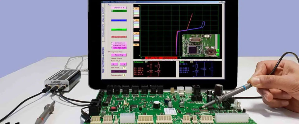
test and validation start with in-circuit or flying-probe test on the bare board and continue with functional test on the assembled unit. Automated optical inspection catches placement and solder defects; X-ray is needed for ball grid arrays and other hidden joints; boundary scan covers nets that cannot be reached with a probe. Environmental testing, thermal cycling, vibration and humidity, is what separates a design that works on a bench from one that survives in the field.
Failures found at this stage are cheap. A defect found after volume production has started is not, which is the argument for testing the design margin rather than only the design function.
Moving to Volume Production
Transition to volume production is mostly about locking the process. The stackup, the materials, the panel layout, the stencil and the reflow profile are frozen and documented, and any change is handled through a change control process with a re-qualification attached. First article inspection confirms that the production line produces what the prototype proved, and ongoing process capability data keeps it that way.
The design decisions that make this transition smooth are unglamorous: generous tolerances, standard materials, panel-friendly outlines, and test access for the nets that matter.
FAQ
Documentation and Change Control
The documents that travel with the board are as much a part of the product as the Gerbers. The stackup drawing fixes the dielectric thicknesses and the copper weights; the impedance table ties each controlled net to a measurement coupon; the assembly drawing shows which parts go on which side and in what order; and the fabrication notes record the surface finish, the tolerance class and the marking requirements. When one of these is missing, the fabricator supplies a reasonable default, and the default may not be what the designer assumed.

Change control is what keeps a release honest. Every revision should carry a revision number, a date, a description of what changed and a note explaining which boards are affected. When a change touches the stackup, the material or the panel layout, the qualification work done for the first article has to be repeated, at least in part, because those three things determine impedance, mechanical behaviour and yield. A change that looks trivial on the schematic can move the impedance of a controlled net by several ohms, and that is exactly the kind of drift that turns a working prototype into a failing production build.
When should the fabricator be involved? Before layout, not after. A five-minute conversation about minimum trace width, layer count and available materials prevents a redesign that costs weeks.
Does a prototype have to use the production stackup? Ideally yes. A prototype built on a different material or layer count validates the circuit but not the impedance, the thermal path or the fabrication yield, which are usually the reasons the prototype exists.
What is the most common cause of a costly redesign? A requirement that was never written down. Controlled impedance, current capacity, height limits and connector positions all need to be stated in the design inputs, because the layout cannot infer them from a netlist.