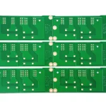
Through, Blind and Buried Vias in PCB Fabrication
A printed circuit board is a stack of copper layers separated by insulating material, and the layers cannot connect to each other on their own. The plated hole that bridges them is the via, and its three forms, through, blind and buried, differ not only in geometry but in when they are drilled and how much they cost. Choosing between them is one of the decisions that most directly sets the fabricator’s process route, so the trade-offs are worth understanding before the stack is fixed.
What a via does
A via is a copper-plated hole that connects conductive patterns on different layers and carries signals or power between them. It is not a mounting hole: no component lead or reinforcing material is inserted into it, and its only job is electrical continuity through the dielectric. As layer counts rise, the number of vias rises with them, and the space they occupy becomes a significant fraction of the routing area. That is why the mix of via types on a board is a density decision as much as a fabrication one.
Through vias
A through via is drilled after the layers are laminated and passes through the entire board, so it is visible on both outer surfaces. It is the simplest form to produce, needs no special lamination sequence, and can be drilled and plated in one pass. The drawback is that it consumes area on every layer it crosses, including layers it does not connect, and the unused portion of the barrel forms a stub that degrades high-frequency performance. In a thick backplane a long through-via stub can be a serious signal-integrity problem, which is one of the main reasons blind and buried vias appear in high-speed designs.

Blind vias
A blind via connects the outermost layer to an adjacent inner layer and stops there, so it can be seen from one side only. Because it does not cross the full board, it frees routing space on the inner layers it never reaches and removes most of the stub. Blind vias sit at the top or bottom surface and have a defined depth, so the drilling operation must land at the correct layer rather than simply penetrate the panel. The depth-to-diameter relationship has to be controlled carefully: if the hole is too shallow the connection is unreliable, and if it is too deep the plating chemistry cannot reach the bottom evenly. An alternative route is to drill the layers that need connecting before the final bond, which requires precise registration equipment but avoids the depth-control problem entirely.
Buried vias
A buried via connects two or more inner layers and never reaches either outer surface. It cannot be produced by drilling a finished board, because the hole is not accessible from outside. Instead the inner cores are drilled, plated and partially bonded first, and the remaining layers are laminated over them afterwards. That extra lamination cycle is what makes buried vias the most expensive of the three, and it is why they are reserved for genuinely dense boards where the space reclaimed on the outer layers justifies the cost. Where density is the binding constraint, the calculation usually favours them anyway. The trade-offs between the available structures are summarised in the guidance on blind and buried via stack selection.
<img src="https://www.gopcba.com/wp-content/uploads/2026/08/rigid-flex-pcb-design-guidelines-1.webp" alt="Via plugging and solder mask filling on a dense circuit board” />
Via plugging options
Once the vias exist, they often have to be sealed. The requirement depends on what happens to the hole afterwards. Three cases appear in practice: a hole that needs nothing but its copper plating, with the solder mask either plugged or left open; a hole that must be filled with solder to a defined thickness, typically around 4 microns, so that solder mask ink cannot enter and form solder balls inside the barrel; and a hole that must be fully plugged with solder mask ink and finished opaque and flat, with no solder ring or solder balls and no light passing through. Which of the three applies is a functional decision, and it should be stated explicitly on the fabrication drawing rather than left to the shop.
Solder mask plugging in practice
Traditionally the mask and the plugging step were handled separately, but a screen-printing approach can complete both in one operation, which makes production more stable and the result more consistent. Whichever method is used, the finished surface over a plugged via must be flat enough for the next process. A via that sits under a component pad, or a tented via on a fine-pitch board, has to be filled and over-plated so that the pad remains planar; otherwise the paste deposit is uneven and the joint suffers. Where a via shares space with a pad, the via-in-pad and plated-through options describe the processing consequences of each choice. Flatness is also an inspection criterion, so the acceptance limits should be defined before production rather than negotiated afterwards.
Aspect ratio and drilling depth
The controlling capability figure for any via is the aspect ratio, the board thickness divided by the drilled diameter. As the ratio rises, the plating bath has more difficulty exchanging chemistry inside the barrel, and the copper in the middle of the hole ends up thinner than at the ends. The consequence is a latent open that passes electrical test and fails under thermal cycling. For blind vias the depth-to-diameter ratio is the equivalent figure, and it is harder to hold because the drill must stop at a specific layer. Drilling is one of the most critical steps in the whole process, since it provides both the electrical connection and, for through-holes, the mechanical anchoring of components; a drilling fault can leave a device that cannot be fitted or a board that has to be scrapped. Confirm both the aspect ratio and the drilling capability against the fabricator’s process before releasing the stack, and check that via clearance to neighbouring copper is adequate, as described in the via to trace clearance rules.
Selecting via types for a design
The decision sequence is straightforward once the constraints are known. Start with through vias, because they are the cheapest and the most robust, and keep them for anything that does not sit in a high-speed path or a dense escape region. Promote a net to a blind via when the stub is unacceptable or when the routing underneath genuinely needs the space. Reserve buried vias for the inner-layer connections that would otherwise force an extra pair of layers, since their cost is only justified when they replace a layer rather than merely tidy one. Then check the result against the fabricator’s capability in both directions: the finished diameter has to be large enough for the plating line to cover the barrel, and the depth or the board thickness has to stay inside the aspect ratio limit. A stack that looks efficient on the layout but exceeds either limit will be re-quoted or re-engineered after release, which is the most expensive moment to discover the problem. Document the via type, the finished diameter and the plugging requirement for every hole class on the fabrication drawing, so that the shop does not have to infer the intent from the artwork. That single piece of documentation removes most of the questions that otherwise arrive after the order is placed.
FAQ
Which via type should I use on a normal four-layer board? Through vias are almost always the right answer at low layer counts. They add no lamination cycles and cost the least, and the stub penalty only becomes significant at high frequencies or on thick boards.
Why do buried vias cost more than blind and through vias? A buried via has to be drilled and plated at the inner-core stage and then covered by an additional lamination cycle. That extra cycle consumes material, press time and yield, so the price reflects the process rather than the hole itself.
Does every via need solder mask plugging? No. Some vias only need their copper plating, while others must be filled with solder or fully plugged and rendered opaque with mask ink. State the requirement on the fabrication drawing, because the process differs for each case.