PCBA Design Mistakes That Raise Assembly Cost
Most of the cost of a PCB assembly is fixed by decisions taken during layout, long before a purchase order is raised. Panel geometry, component choice, the number of part types and the surface finish all determine how difficult the build is, and difficulty shows up as rework, slower throughput and a higher unit price. PCBA design mistakes are rarely dramatic; they are small choices that multiply across a production run.
Bring the Assembly Partner In Early
The first mistake is timing. An assembly partner should see the layout while the first draft is still editable, and there should be enough schedule left for a prototype build and a pilot run before the design is frozen. Checks performed on paper or in the CAD system cannot reveal every problem; some issues appear only when the first boards are built, and the components for the first planned production build must be ordered with those findings already incorporated.
Getting an expert opinion at the draft stage costs a meeting. Getting the same opinion after the tooling, the stencil and the purchase orders exist costs a revision, and it can put a launch date at risk.
Panelization Is Not a Detail
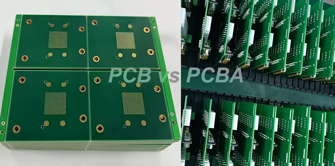
The correct panel depends on the processes the board and its components will go through. A panel that is too large or too small for the line will not run reliably. Very thin boards, around 0.8 mm and below, often need a smaller panel to prevent bowing, while a panel without enough waste material on the edges can be difficult to handle during production and test.
Breakaway design matters just as much. Tabs that are cut in the wrong place leave the assembly too flexible, or make separation difficult without stressing components. Missing fiducials cause alignment errors that appear as placement offsets. The practical approach is to let the assembly partner work with the board supplier on the panel layout, so the result satisfies both the fabrication and the assembly process.

Once the panel is right, the design content itself becomes the cost driver.
Complexity Costs Twice
Placing surface mount components on both sides of the board is significantly more expensive than single-sided assembly, because the board must be processed twice, with an extra set of stencils, programs and handling steps. It usually costs close to double. The same applies to through-hole parts, which require a separate soldering operation and often manual work.
The cost is not only in the assembly. Double-sided placement constrains the reflow sequence, limits the thermal profile that can be used, and adds a second opportunity for defects. Where double-sided assembly is genuinely required, the layout should concentrate the second side into a small area, so the extra pass is short.
Component Sizes, Shapes and Pad Fit
Every component on the bill of materials should be checked against the pad it will be soldered to, including the body dimensions and not only the lead spacing. A part that is electrically correct but physically larger than the space allowed will interfere with a neighbour, and a part placed too close to the board edge can be damaged during separation or machining.
Mixed component sizes create a subtler problem. Placing very small components next to large ones that need more paste forces a compromise in the stencil design, and the compromise often means an extra step stencil, which raises cost. Grouping similar sizes together lets the stencil be optimised for one paste volume.
Vias in Pads and Solder Mask Openings
Putting a via in pad looks like a way to save space, and it is a way to lose solder. During reflow the paste wicks into the barrel and the joint is left short. If the via must be in the pad, it has to be filled and plated over so the surface is flat.
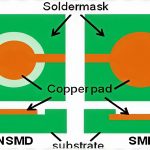
Solder mask openings deserve the same attention. Pads that are placed very close together can share solder and produce a bridge, and on fine-pitch devices a thin mask dam between pads may not survive the process. Thinking about where the solder will flow, and leaving a mask web where it is needed, is cheaper than reworking shorts. These are the same principles that apply to manufacturability in general.

The bill of materials then determines how much of the assembly cost is fixed before the first board is placed.
Part Count and Part Variety
Every additional part type adds a feeder, a reel, a placement program entry and an incoming inspection step. Reducing the number of distinct part numbers, even where it means using a slightly larger or less precise component, usually lowers total cost more than the component price difference suggests. Removing unnecessary parts has the same effect.
Test points and programming headers are the obvious candidates once a product moves beyond prototyping. They are necessary during development and often redundant in production, where functional test is performed through a connector. Reviewing them at the transition from prototype to production is a straightforward saving.
Surface Finish Choices
The surface finish has to suit the components, not the purchasing preference. A standard tin-lead finish is not the right choice for fine-pitch assembly, and the various alternatives differ in shelf life, flatness and cost. Where the assembly involves fine-pitch parts, a flat finish such as immersion gold is normally required, and where the boards will be stored for a long time before assembly, shelf life becomes a selection criterion.
Changing the finish later is possible but it invalidates the process assumptions that were made for the original. Choosing the finish with the assembly partner, in the light of the component mix and the storage plan, avoids the retrofit.
A finish that is chosen for cost alone can also raise cost in a different place. A finish with a shorter shelf life forces the boards into assembly sooner, and one with poor flatness forces a compromise in the stencil. Comparing finishes on total programme cost, including storage and rework, gives a different answer from comparing the price per square metre, and the board quality characteristics that matter to assembly usually decide the outcome.
Component Placement Near Edges and Neighbours
Components placed too close to the edge can be damaged when the panel is separated, and parts placed too close together can be disturbed by the placement nozzle. Parts that are much taller than their neighbours can shadow them during reflow, and parts mounted under a large component create a rework problem because the large part must be removed first. These are layout decisions, and the placement order and pad positioning review is where they should be caught.
The review is also the moment to check marking. Component reference designators must be visible enough for inspection, and polarity marking must be conventional, because the placement program is generated from the designators and an operator needs to verify orientation against the drawing.
FAQ
When should the assembly partner see the layout? While the first draft is still editable, with enough schedule remaining for a prototype and a pilot build. Feedback after the design is frozen is much more expensive to act on.
Why is double-sided SMT so much more expensive? The board must pass through the line twice, with two stencils, two programs and two reflow cycles, and the second pass adds handling and defect risk. The cost is typically close to double.
Is a via in a pad ever acceptable? Yes, if the via is filled and plated over so the pad surface is flat. An open via in a pad wicks solder away from the joint during reflow.