PCB Prototype Production Flow: Cutting, Drilling and Plating
A prototype order moves through the same production line as a volume order, but with different economics. Setup dominates, quantities are small, and the process has to be flexible enough to handle a design that has never been built before. Understanding the flow makes it easier to write a data package that moves quickly and to know which requests are reasonable and which will slow the order down.
Before the Panel Is Cut
PCB prototype production begins with the data review. The fabricator checks that the artwork, the drill file, the stackup and the fabrication notes agree with each other, and raises a question if anything is ambiguous. This step is short when the package is complete and long when it is not, which is the main reason two similar designs can have very different lead times.
A complete package includes the copper layers, the solder mask and silkscreen, the drill file with its tool sizes, the outline, the stackup with dielectric thicknesses, the impedance targets and the finish. Anything missing becomes an assumption.
Panel Cutting and Edge Preparation
The laminate is cut from a larger sheet to the panel size required by the order, which is chosen so that the boards fit with their rails and fiducials. A panel that is too narrow for the machine or too large for the press will be rejected at this point, which is why the outline and the panel arrangement are usually agreed before the order is placed.
The cut edges are then deburred and rounded. A sharp corner on a panel catches on rollers during processing, and the resulting damage is a scratch or a crack that appears much later as a defect.
Drilling
Holes are drilled on a CNC machine using a programme derived from the drill file. The parameters depend on the hole diameter, the laminate and the aspect ratio, and tool life is counted in hits because a worn bit heats the hole wall and smears the resin.

Registration at this step is what determines whether the drilled holes land inside their pads. Entry and exit material control burring, and a deburring step follows rather than brushing, which would round the copper edges and change the line width.
Electroless Copper
The drilled hole walls are not conductive, so a thin layer of copper has to be deposited chemically before electroplating can build the barrel. This is the electroless copper step, and it begins with a desmear process that removes the resin smear left by drilling and prepares the surface for the subsequent chemistry.
Activation follows, which deposits a catalyst on the hole wall, and then the electroless bath deposits a thin copper layer over the entire surface including the hole walls. That layer is only a fraction of a micron thick, but it is what makes the panel conductive and allows the electrolytic plating step to work.
Pattern Transfer
pattern transfer moves the image from the film onto the panel. In the dry film process, a photoresist is laminated to the copper, exposed through the artwork and developed so that the resist remains where copper is wanted. In the older screen printing process, an etch resist is printed directly. Either way, the result is a panel where the copper to be kept is protected and the copper to be removed is exposed.
Registration between the image and the drilled holes is the critical parameter. On a fine-line design the accumulated tolerance from lamination, drilling and imaging is what limits the minimum annular ring.
Pattern Plating and Etching
pattern plating builds copper on the exposed conductors and the hole walls to the specified thickness, and it deposits the metal layers that will form the surface finish, such as nickel and gold or tin. Because the plating current density varies across a panel, the thickness has to be verified inside the holes as well as on the surface.
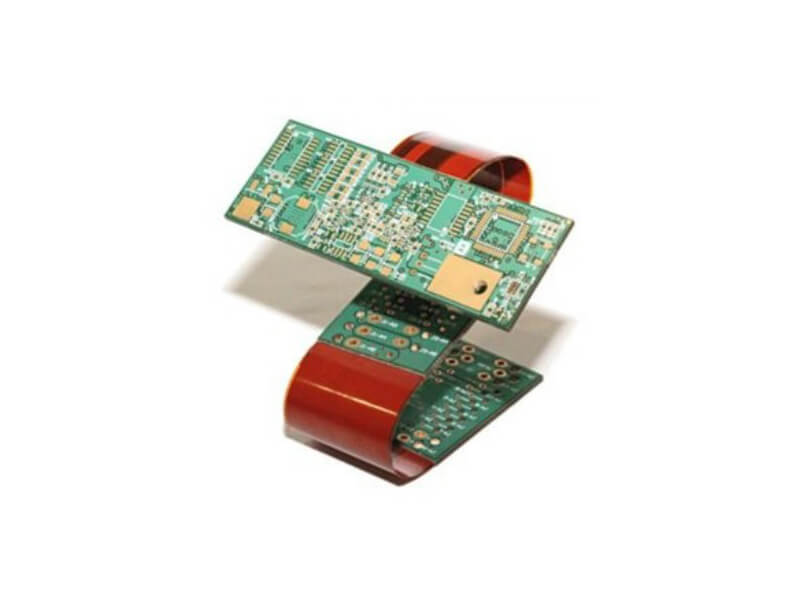
The resist is then stripped and the thin seed copper between the plated features is removed in a short flash etch. That etch is deliberately brief, because the plated features are already at their final width and additional etching would close the gaps that define the fine lines.
Why Small Batches Are Different From Large Ones
A prototype panel spends more time in setup and less time in running than a production panel. The tooling, the programme and the first article checks are the same cost regardless of the quantity, which is why the price per board falls steeply with volume and why changes after the first build are expensive out of proportion to their size.
It also means that the decisions made before the first order have more leverage than anything decided afterwards. Layer count, stackup, minimum features and the finish are all easier to get right at the start.
Getting the Order Through Quickly
Solder Mask, Finish and Profile
After the copper is complete, the panel is coated with solder mask, which is imaged to expose the pads and cured. The finish is applied next, chosen for the assembly process and for the storage life the product needs, and it is applied selectively where a connector tab needs a hard gold surface rather than a solderable one.
The profile comes last. The boards are routed from the panel, and the panel scheme determines how cleanly they separate and how much handling they see before packing. A prototype that is delivered as loose boards has been handled more than the same design delivered in an array, which matters for a thin board or one with a narrow neck.
Electrical Test and Documentation
Bare board electrical test verifies continuity and isolation on every net, which on a prototype is normally done with a flying probe because there is no fixture. Impedance coupons are measured where the design has controlled-impedance nets, and the results should be recorded against the stackup rather than merely checked as pass or fail.
The panel also generates documentation: the test record, the coupon measurements and any deviation that was agreed. For a prototype that will be followed by a production order, that record is the baseline against which the production build is compared.
Speed comes from completeness rather than from urgency. A package with a clear stackup, a consistent drill file and an explicit fabrication note moves through the data review in minutes. A package with a drilled hole in one file and no corresponding pad in another generates a question, and every question costs a round trip. Multilayer PCB prototype requirements lists what to provide, and PCB design and fabrication working together covers the interfaces where mistakes usually happen.
From Prototype to Assembly
Most prototype orders are followed by an assembly order, and the two are easier to plan together. If the boards will be assembled, the panel scheme should leave room for the stencil, the fiducials should be visible to the placement machine, and the outline should allow the boards to be depanelized without stressing the parts. PCBA development process covers the sequence that follows fabrication.
FAQ
Why is a prototype so much more expensive per board than a production run? Because setup, tooling and first article inspection are fixed costs. They are spread across the whole order, and a small order has few boards to absorb them.
Can a prototype be built on different materials from production? It can, but the impedance, the thermal behaviour and the assembly results will differ. If the prototype exists to validate performance, use the production stackup.
What slows a prototype order down most often? Missing or inconsistent data, especially drill files that do not match the pads, and stackups that do not specify the dielectric thickness required for the impedance targets.