




PCB Routing Techniques That Improve Manufacturability
A layout can be electrically correct and still be difficult to build. Manufacturability problems do not show up in a simulation, and they do not show up on the bench prototype, because the prototype was made with extra care. They show up in production, where the process runs at its normal tolerances and the design has to work anyway.
Trace Width and Current
Trace width is chosen for current capacity first and for impedance second. A signal trace that carries only a logic level can be drawn at the process minimum, while a power trace must be sized against the current it will carry and the temperature rise that is acceptable.
The mistake that appears most often is a power net routed at signal width because it looked adequate on the schematic. Checking width against current during routing, rather than after the layout is finished, avoids a late redesign of the whole power path.
Spacing Rules and Their Purpose
Minimum spacing is set by the fabrication process, and it applies to copper to copper, pad to trace and copper to board edge. Each of these has a different origin: the copper to copper limit comes from etching, the board edge limit from routing, and the pad to trace limit from solder mask registration.
Solder mask adds a constraint that is easy to miss. The mask opening is larger than the pad, so two pads that are electrically far apart may still violate the mask web minimum. That web is what prevents solder bridging, and ignoring it produces a board that passes design rule checking and fails in assembly.
Via Placement
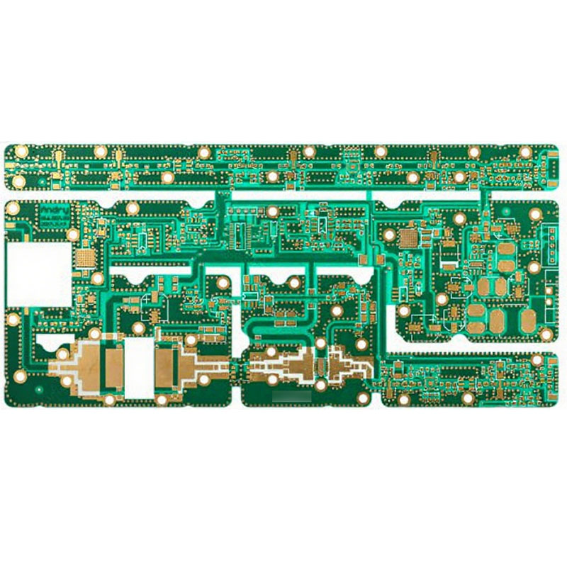
Vias take space on every layer they pass through, and they interrupt the planes they cross. Grouping them rather than scattering them keeps the planes continuous and gives the return current a clear path around the cluster.
Via size and annular ring follow the same rules as component holes, and the same tolerances apply. Where a via is placed in a thermal pad, the paste volume and the via filling or tenting must be decided deliberately, because an unfilled via in a pad wicks solder away from the joint. The interaction between vias and thermal pads is described in our pad and hole size article.
Copper Balance
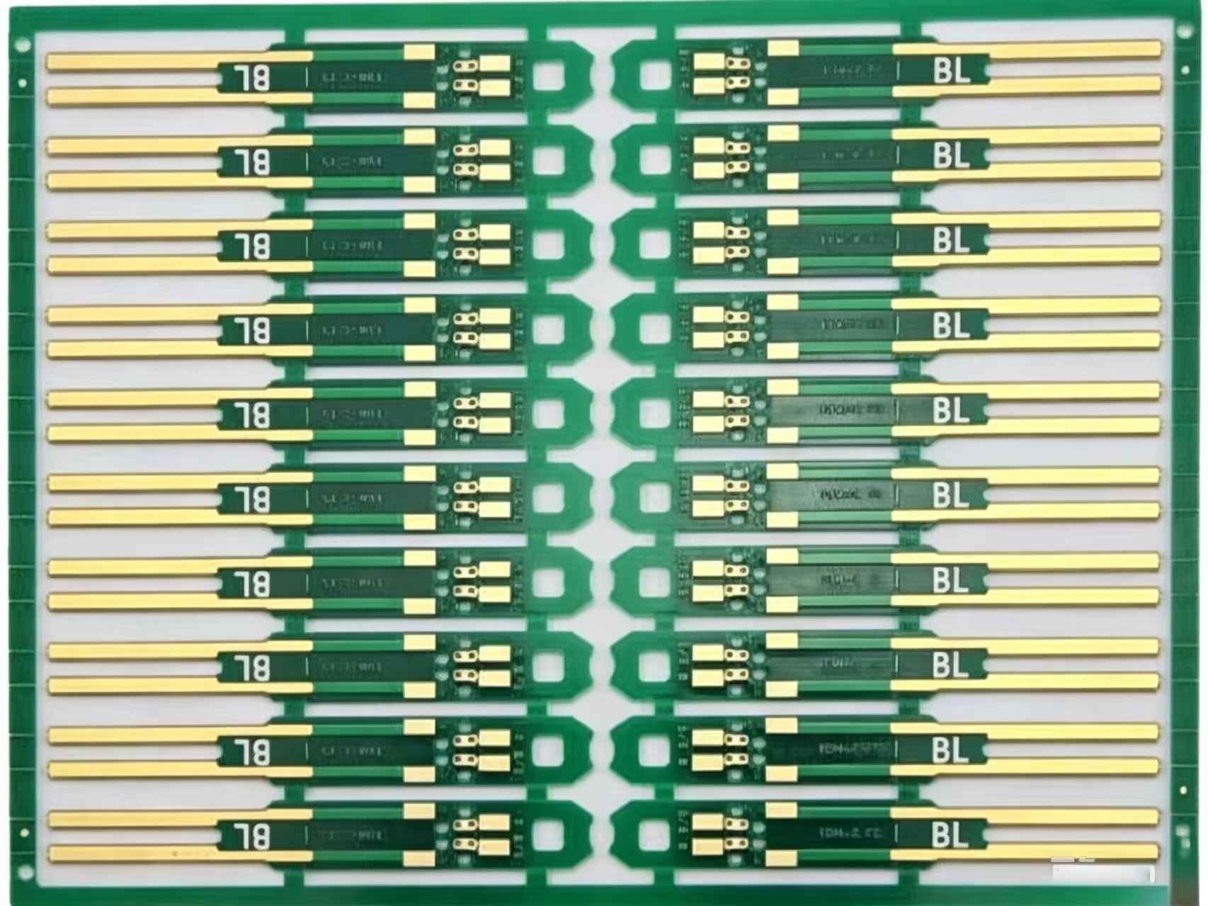
Uneven copper distribution across a layer causes uneven etching, uneven plating and uneven heat during assembly. A region with almost no copper etches differently from a dense one, and the resulting trace widths vary across the board.
Adding a thieving pattern or a ground pour to sparse areas balances the distribution. The pour should be connected rather than floating, because an isolated copper area is a stray capacitance and a potential antenna, and it should be checked against the same spacing rules as the rest of the copper.
Component Placement for Assembly
Routing cannot compensate for bad placement. Components should be oriented consistently, spaced so that a nozzle can reach them without colliding with a neighbour, and arranged so that the paste printing and the reflow profile can be uniform.
Large components next to small ones create a thermal imbalance during reflow, because the large part absorbs heat and the small one reaches temperature first. Grouping components of similar thermal mass, and separating the extremes, is a placement decision that improves both yield and joint quality. The assembly consequences are covered in our PCBA soldering requirements article.
Testability
Test points should be placed during the layout, not added afterwards. A board with no access to its nets can only be tested functionally, which means a fault is attributed to the product rather than to a specific joint.
The test points need clearance for the probe, and they should be on a single side where possible to keep the fixture simple. A board with test points on both sides needs a more complex fixture and costs more to test, which is a design decision rather than a manufacturing one.
Checks Before Release
The final check should compare the layout against the fabricator capability, not against a generic rule set. A design that meets the capability of the supplier who will build it is manufacturable, and one that meets a stricter rule set may simply be more expensive than it needed to be.
Alongside that, running a silkscreen review and a footprint review catches the errors that design rule checking cannot see. A release checklist makes the process repeatable, and it is what allows a design to be handed over without a series of clarifications.
Routing Techniques That Scale With the Board
The techniques that work on a small board do not always survive a larger one. Longer traces change their electrical behaviour, a larger area allows more variation in etching and plating, and the assembly process sees a bigger thermal mass.
Scaling up therefore means revisiting the assumptions rather than extending the layout. A trace that was electrically short on the prototype may need impedance control in the product, and a spacing rule that was comfortable on a small panel may be marginal on a large one. The electrical consequences are covered in our high speed routing notes.
Running a DFM Check
A design for manufacture check compares the layout against the rules the process actually uses, and it should be run with the fabricator capability rather than a generic rule set.
The check catches the violations that design rule checking ignores: solder mask webs that are too narrow, silkscreen printed over a pad, test points that are covered, and copper too close to a route path. Each of these is cheap to fix in the layout and expensive to discover on a panel. Our stencil requirements article describes the printing constraints that the same check should include.
Handing Over the Design
Manufacturability also depends on what travels with the design. The fabrication drawing, the assembly drawing, the drill file and the stackup should all be consistent and revision controlled.
A layout that is correct but undocumented will be built to whatever the manufacturer infers. Documenting the requirements is what makes the manufacturing outcome repeatable, and it is the last routing technique worth mastering.
Where the design is handed to a partner rather than built in house, the same package supports the review. A manufacturer who receives the requirements with the data can raise questions before the panel is committed instead of raising them after.
Reviewing the layout against the assembly process is part of the same exercise. Nozzle clearance, panel support and the orientation of connectors all affect yield, and each is visible in the layout long before a panel is produced.
FAQ
Is a ground pour always beneficial? It helps with copper balance and can provide a return path, but only if it is properly connected. A floating pour adds capacitance and can worsen emissions.
How many times should a layout be reviewed? At least once by someone other than the designer, specifically against the manufacturing rules. Most manufacturability problems are visible to a fresh reader in minutes.
Can design rules be relaxed to save cost? Sometimes, for a board with no fine features. The saving is small, and the risk of a yield problem is real, so it is rarely worth doing on a complex board.



1 Comment
Rigid PCB Structure and How It Works
[…] because an isolated copper island adds stray capacitance without contributing anything else. Our routing techniques article covers the same practice from the manufacturing […]