Double-Sided PCB: Definition, Structure and Applications
A double-sided pcb occupies an unglamorous middle position in the market, and that is exactly why it ships in such volume. It costs far less than a multilayer stackup and offers far more routing freedom than a single-sided board, so it lands in the sweet spot for consumer products, industrial controllers and automotive modules. Understanding where its limits lie prevents a design from being pushed into a four layer board unnecessarily.
What Defines a Double-Sided Board
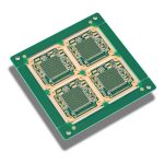
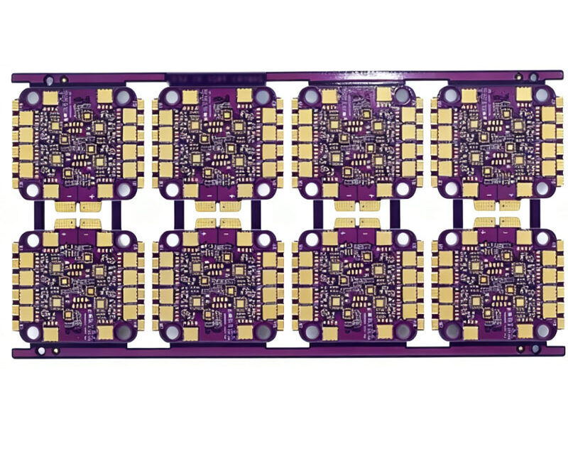
A double-sided board carries conductive layers on both faces of a single insulating core. Components can be mounted on either side and traces can run on both, with electrical connection between the two faces made through plated through hole barrels. Because both surfaces are available for routing, the same board outline can support roughly twice the interconnect of a single-sided design.
The core is the same laminate used in multilayer boards, and the plated barrels are formed by drilling, electroless copper deposition and electroplating. Once the two faces are connected, the board behaves as a single electrical system rather than two independent circuits, and the designer gains the ability to route a signal on the top layer, cross the plane through a via, and continue on the bottom.
Base Materials and Copper Weight
The substrate is normally woven glass fabric bonded with epoxy resin. Common laminate grades include FR-4 and the paper or composite based FR-1, FR-2, CEM-1 and CEM-3 materials, which trade some electrical and mechanical performance for lower cost. An FR-4 substrate remains the default because its dielectric behaviour, dimensional stability and moisture resistance are predictable across a wide range of processes. Composite grades are chosen where the circuit is simple and cost sensitive, and their mechanical strength and thermal limits are correspondingly lower.
Copper thickness is specified by weight rather than by dimension, and the practical range runs from 1 ounce, about 35 micrometres, up to 6 ounces, about 210 micrometres. Heavier copper is used where the trace has to carry current or where heat has to be spread laterally. Any increase in copper weight also changes the etch behaviour, so minimum trace and space must be relaxed as the foil gets thicker.
Surface Finishes Available
The copper that will be soldered has to be protected from oxidation between fabrication and assembly. An organic solderability preservative is the cheapest option and gives a flat surface, but its shelf life is measured in months and it is sensitive to repeated thermal cycles. Hot air solder levelling, known as HASL, is the most widely available and most forgiving finish, though the surface is not perfectly flat.
Electroless nickel immersion gold gives a flat, durable surface that suits fine pitch and press-fit parts, at a higher cost. Immersion silver and immersion tin offer flat surfaces at moderate cost with their own storage constraints. Where the finish is also the contact surface, as on a gold finger edge connector, hard gold plating over nickel is used because it resists the wear of repeated insertion, covered in lead-free versus leaded solder.
Dimensional and Manufacturing Limits
A typical two layer board can be built from 0.4 mm to 3.2 mm in total thickness, with the panel size reaching roughly 510 mm by 650 mm before routing. Minimum trace width and spacing of about 0.10 mm are achievable in volume, and minimum drilled hole diameter sits between 0.2 mm and 0.3 mm, with a minimum annular ring and hole to copper clearance near 0.127 mm.
Those numbers describe what a capable fabricator can hold rather than what any given design should use. Pushing to the minimum on every net increases the scrap rate and the price, and it leaves no margin when the design has to be revised. Most two layer designs are better served by 0.15 mm traces and 0.25 mm holes, which cost less and rework more easily. It is also worth checking the fabricator panel utilisation before squeezing the geometry, because a board that fits the standard panel with ordinary rules is often cheaper than one that needs a special process step.
Routing Density and Board Area
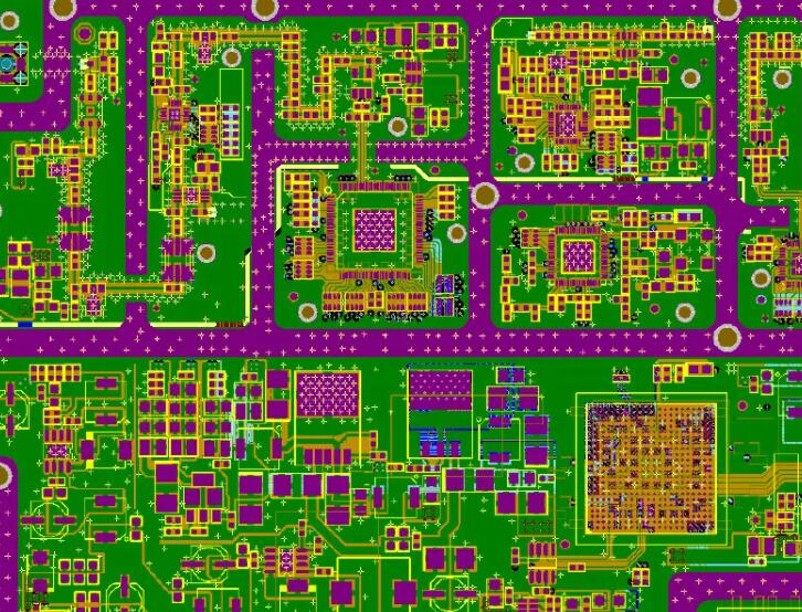
The value of the second layer is not only extra routing area. It is the ability to place a continuous ground or power region on one side without consuming the other side entirely, which lowers the impedance of the return path and improves immunity. A two layer design with a nearly solid bottom ground and signal routing on top often outperforms a poorly planned four layer board.
Where the density exceeds what two layers can carry, the answer is usually to move up to four layers rather than to shrink the geometry further. A four layer stackup adds a dedicated ground plane and a power plane, and the resulting improvement in return path and plane capacitance is worth more than the extra cost in most high speed designs. The design choices behind that step are set out in PCB circuit board explained.
Applications That Fit Best
Consumer electronics make up the largest share: televisions, appliances, power adapters and simple control boards all sit comfortably on two layers. Computer and network equipment uses them for interface boards and peripheral cards, while industrial control systems rely on them for I/O conditioning, relay drivers and instrumentation front ends, where the circuit is wide rather than fast.
Automotive electronics use double-sided boards for body control modules, sensor interfaces and navigation units, where robustness and thermal cycling matter more than trace density. Portable medical monitors and diagnostic instruments follow the same pattern: the circuit is moderately complex, the volumes are real, and the cost of a four layer board cannot be justified by the performance gain.
Design and Fabrication Workflow
The workflow begins with the schematic, where component selection, current and voltage distribution and power dissipation are settled. Layout follows, and the objective there is to place components so the signal paths are short and the return currents stay under their own traces rather than wandering across the board. Ground and power regions are then poured and stitched.
Verification comes next: a design rule check against the fabricator capability, an electrical rule check for open and short conditions, and simulation where signal integrity or thermal behaviour is in question. Fabrication then runs through imaging, etching, electroless copper, plating, drilling and finish, followed by functional testing on the finished board, with the plated barrel construction described in via in pad or plated through.
FAQ
Can a double-sided board carry a controlled impedance trace? Yes, if the fabricator has a known dielectric thickness and the trace geometry is defined against a solid reference plane on the opposite side. The tolerance is wider than on a multilayer stackup, so impedance controlled nets on two layers are best kept to loose targets.
Is a two layer board cheaper than four layers by a large margin? Material and processing both drop, but the difference depends heavily on quantity and panel utilisation. At low volume the gap can be small, while at high volume the two layer board is markedly cheaper per unit.
Should both sides carry components? Mixed assembly on both faces is common and does not change the board itself, but it adds a second reflow pass and requires adhesive or a carrier for the underside parts. Single-sided placement is simpler whenever the layout allows it.