Base Station PCB Design: Loss, Layers, and Materials
Wireless infrastructure is built on boards that behave like radio equipment rather than like digital hardware. A base station PCB manages radio-frequency signals at gigahertz frequencies, keeps insertion loss to a minimum, and holds the whole radio chain stable over years of continuous operation. The requirements that follow from that are different from those of a consumer board, and they start with the material.
What makes these boards different
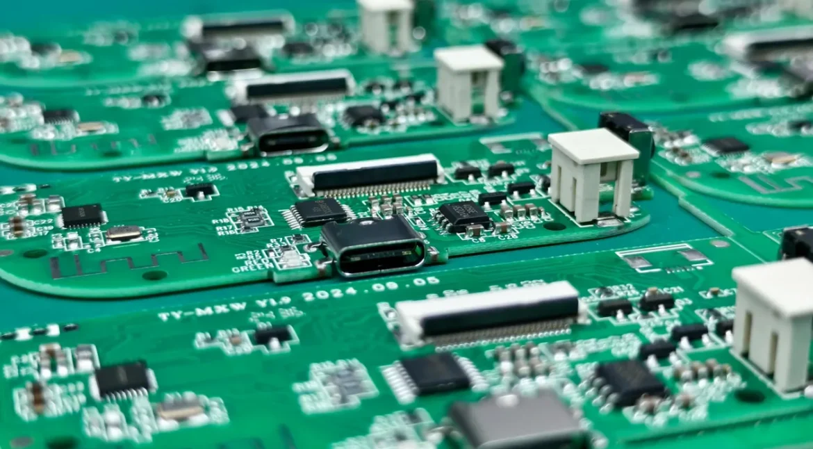
A base station board is designed to carry radio-frequency and microwave signals, which means extremely low signal loss and tight control of electromagnetic behaviour. It appears in transmitters, remote radio units, and antenna modules, and it is one of the components that determines whether a network link holds its performance in service.
A consumer board that loses a little signal merely runs warmer. A radio board that loses signal reduces the link budget, and there is no way to recover that loss once the board is built.
The defining characteristics
Operation at gigahertz frequencies is the first characteristic, driven by 5G and the work now underway for the next generation of networks. Low-loss materials are the second, since the dielectric loss of an ordinary laminate becomes significant at these frequencies.
Multilayer construction is the third. Stacks of eight to twenty layers are common, because the board has to combine radio-frequency sections with digital control and power distribution in a compact volume. Thermal management completes the list: high-power devices need thick copper and thermal vias to move heat into the structure rather than into the surrounding air.
The material choice on a radio board is not a cost decision that can be deferred. Loss is fixed by the laminate, and it cannot be recovered in layout.
Materials
Three classes of material cover the range. Standard FR-4, with a dielectric constant near 4.5, serves low-frequency, cost-sensitive designs and remains adequate for the control sections of many products. Hydrocarbon ceramic laminates, with a dielectric constant around 3.5, are the common choice for mid and high-frequency communication equipment because they balance loss against cost. Polytetrafluoroethylene materials, with a dielectric constant between roughly 2.1 and 2.6, occupy the top of the range and are used where frequency stability and minimum loss are the dominant requirements.
The cost gap between the classes is substantial, which is why a radio board is often built as a hybrid: low-loss material in the radio sections and a conventional laminate in the digital and power areas, joined in the same stack.
Where these boards are used
Macro and small cells form the largest application, since both depend on radio performance in a compact enclosure. Satellite communication ground stations use the same class of board where link margin is critical, and remote radio heads apply it at the point where the digital baseband meets the antenna. Microwave backhaul equipment, which connects a site to the core network, completes the group.
All of those applications combine three requirements: controlled impedance, low loss, and long-term environmental stability. That combination is what separates a base station board from a general-purpose radio board rather than the frequency alone.
Design points
Impedance control is continuous rather than selective. A typical target is 50 ohm, with 75 ohm used in some video and instrumentation interfaces, and the target has to hold across the whole board, because a radio path that changes impedance at a transition loses the margin the material was chosen to provide.
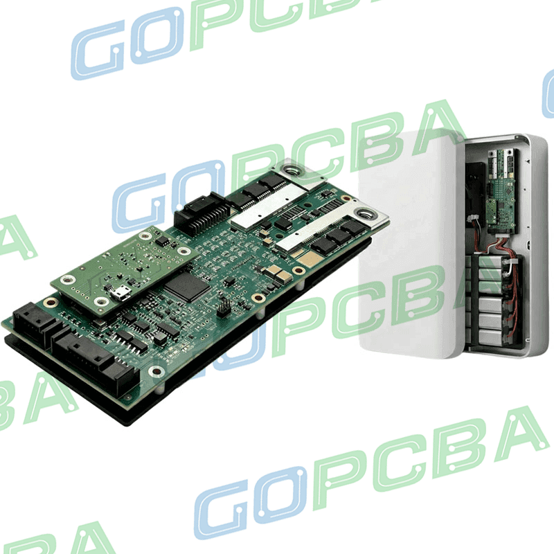
Electromagnetic shielding matters in dense designs, where radio sections sit beside digital control logic. Thermal management relies on thermal vias and copper area to move heat out of power devices rather than letting it accumulate in the laminate. Copper weight of one to three ounces supports the current and the thermal path, and the layout keeps the radio and analog regions physically separate from the digital section so that crosstalk does not have to be filtered out. The trace geometries that make that separation work are covered in our guide to high frequency traces and data bus routing.
On a radio board, isolation is a layout decision. Once two regions share a reference and a neighbourhood, no filter recovers the isolation that placement gave away.
Manufacturing challenges
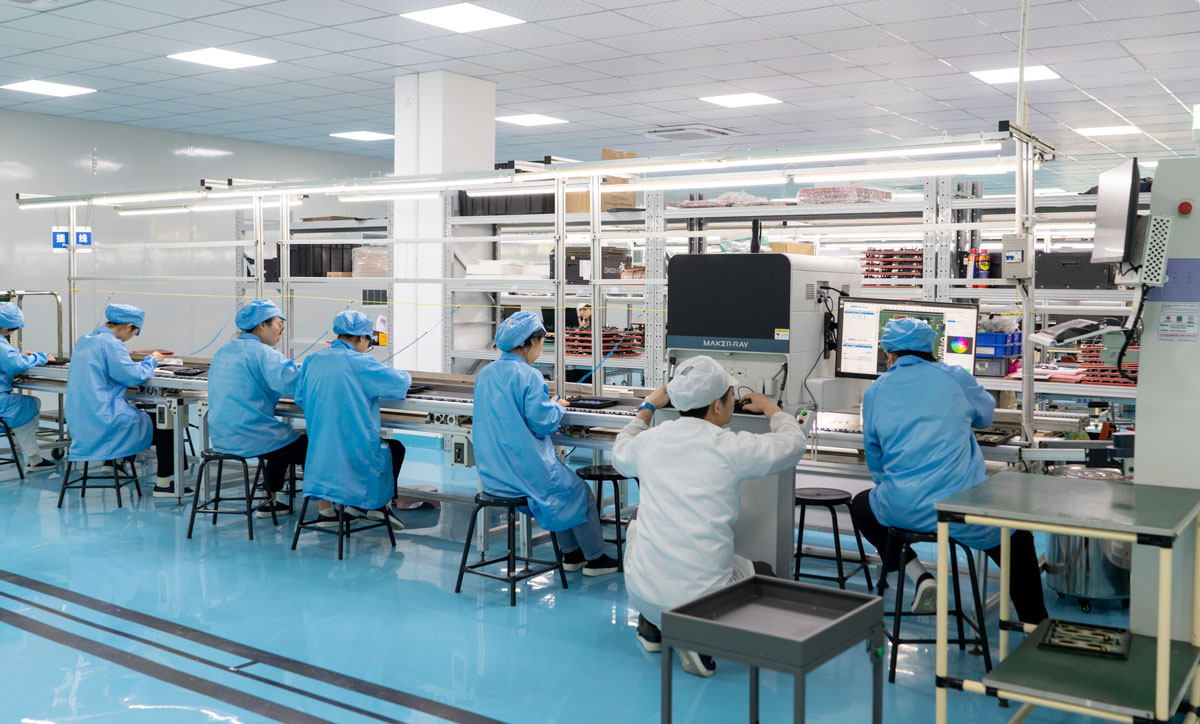
Polytetrafluoroethylene materials are the hardest to process. They drill differently from epoxy laminates, and an incorrect parameter produces smearing or delamination at the hole wall. Multilayer registration is the second challenge, because a stack of eight to twenty layers has to hold alignment across every lamination cycle. Surface roughness is the third, since a rough copper surface increases insertion loss in a way that only appears at high frequency.
The usual responses are precision drilling with parameters developed for the specific material, laser-drilled microvias where density requires them, and a surface finish chosen for both assembly and loss. Electroless nickel electroless palladium immersion gold and immersion silver are both used, with the choice driven by the assembly process and the electrical requirement. The stripline and microstrip geometries that set the impedance targets are described in PCB routing with microstrip and stripline.
Cost structure
The material class dominates the price. A low-frequency laminate sits at the bottom, a mid-range low-loss laminate costs substantially more, and a PTFE-based construction costs more again. Layer count comes next, since an eight-layer stack and a twenty-layer stack are different manufacturing undertakings rather than points on the same scale.
Surface finish adds a smaller premium, ranked from an immersion silver finish through immersion gold to the palladium-containing finishes used for the most demanding assemblies. Quantity then moves the unit price as it does for any board, and the remaining variable is lead time: a complex radio board typically needs one to three working weeks, because the process steps cannot be compressed without risk.
Selecting a supplier
Four capabilities separate the suppliers who can build these boards from those who cannot. The first is certification and documented quality systems. The second is experience with high-frequency and microwave processes, because the parameters that work on FR-4 do not transfer to low-loss materials.
The third is measurement: controlled impedance requires the ability to verify it, and radio boards benefit from radio-frequency test capability rather than electrical continuity alone. The fourth is continuity of supply from prototype through volume, since requalifying a supplier mid-programme is more expensive than choosing one who can scale. The wider question of how layout affects emissions is covered under EMI reduction through stackup and layout.
FAQ
How does a base station PCB differ from an ordinary radio board? It is designed for higher frequency, a more complex multilayer structure, and better thermal and interference performance, because the equipment operates continuously and the link budget has no spare margin.
Can the design be prototyped before production? Yes, and it should be. Low-volume prototype runs allow the impedance and loss behaviour to be measured before tooling and volume commitments are made.
How long does manufacturing take? Between one and three working weeks for a typical stack, depending on complexity, material availability, and the test requirements. Radio boards are not a good candidate for schedule compression.
Which material offers the best value? A mid-range low-loss laminate with a dielectric constant near 3.5 is the usual compromise for 5G work, because it delivers the loss performance the band requires without the cost of a fluoropolymer stack.