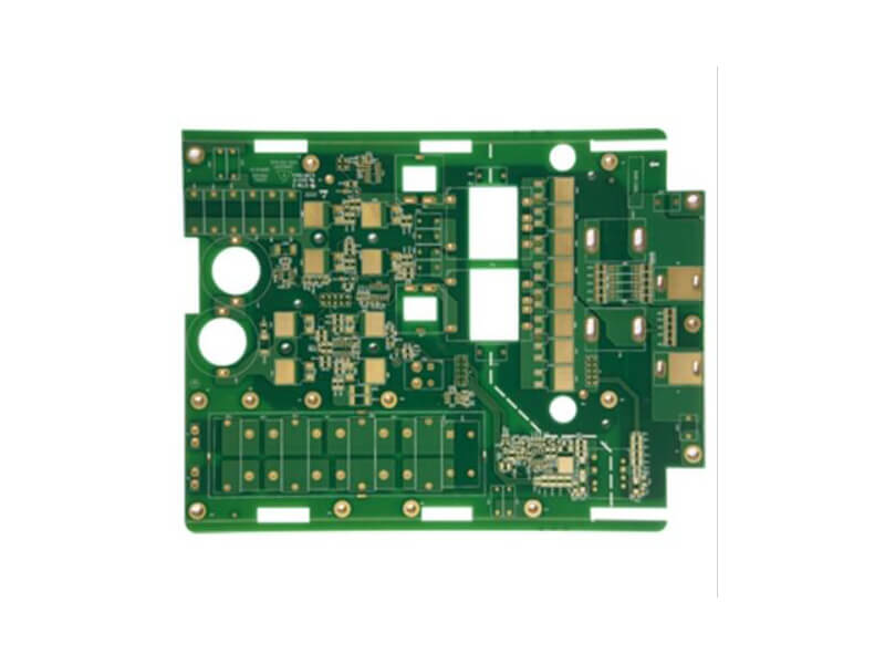
18 Layer PCB: Stackup, Lamination and Design Rules
An eighteen layer board is not simply a bigger version of a six layer board. The layer count changes the fabrication process, the tooling, the achievable yield and the way the stackup is planned, and it introduces failure mechanisms that only appear at high layer counts.
Why Designs Reach Eighteen Layers
Layer count grows when routing demand, power distribution and signal integrity requirements cannot be met with fewer layers. A dense backplane with multiple high-speed buses, a telecom line card or a large switching fabric will reach that range because the signal layers alone require more than a dozen, and each group of signals needs planes beside it.
Beyond roughly ten layers, the count is usually driven by the ratio of signal layers to plane layers rather than by an absolute need for routing space. Two routing layers between each pair of planes is the standard arrangement, and that ratio sets the total.
Stackup Planning at High Layer Counts
The stackup is defined by function. Signal layers are arranged in pairs, each with a reference plane, and the pairs are separated by the core and prepreg schedule that gives the required dielectric thickness. Power planes are placed where they are needed for distribution and, where possible, paired with a ground plane to create distributed capacitance.
Symmetry becomes critical. With eighteen layers there are more interfaces to constrain, and an unbalanced schedule accumulates stress across the whole stack. The fabricator’s capability for residual copper balance and thickness tolerance is a real limit on what can be built reliably.

Lamination Cycles and Registration
High layer counts are usually built with sequential lamination, in which sub-assemblies are pressed together in stages. Each stage adds registration error, because every press cycle moves the material slightly, and those errors accumulate toward the outer layers.
Design rules account for this with larger annular rings on outer layers and generous clearance between features on different layers. The designer who applies a six layer assumption to an eighteen layer board will produce a design that is unbuildable at any reasonable yield.
Aspect Ratio and Drilling
Plated through holes in a thick stack reach high aspect ratios, and plating uniformity inside a deep barrel becomes the limiting process capability. Sequential lamination addresses this by allowing buried and blind vias, so that the deepest hole that must be plated is shallower than the finished board thickness.
Drill accuracy also changes. With more layers to align, mechanical drilling has to hold position across a long stack, and laser-drilled microvias on outer layers must register accurately to the inner structures created in earlier lamination cycles.

Materials and Thickness Tolerance
The total finished thickness is the sum of many individual layers, each with its own tolerance. As the layer count rises, those tolerances accumulate, and the impedance of a controlled trace depends on the dielectric thickness beneath it.
Two responses are standard. The first is to specify impedance control with coupons and to measure rather than assume. The second is to define the dielectric thickness for critical layers and let the fabricator adjust the prepreg schedule elsewhere to achieve the overall thickness.
Thermal and Mechanical Behaviour
A thick board is stiffer and heavier, and it expands more in the z-axis during reflow. That expansion is what stresses plated barrels, and the effect is cumulative, so a high layer count board benefits disproportionately from a high glass transition temperature laminate.
Weight and stiffness affect assembly as well. The board may sag during reflow unless it is supported, and the panel may need a different carrier or conveyor configuration. These are production considerations that should be discussed with the fabricator during design rather than after the first order.
Cost and Yield
Cost rises faster than linearly with layer count. Material, lamination cycles, drilling steps, inspection and the accumulated yield loss at each stage all contribute, and the yield effect is the largest term because a defect at any stage affects a board that already contains many hours of processing.
Reducing the layer count by improving routing efficiency, using finer lines within the fabricator’s capability or moving some functions to a separate board often saves more than it costs. The decision should be based on total system cost rather than on the layer count in isolation.
Design Rules That Matter Most
Define all layers explicitly, including plane layers and any internal routing. Maintain a continuous reference for each high-speed signal across its whole length, and account for the registration tolerance when setting via and pad geometry.
Then verify the design against the fabricator’s actual capability rather than a generic rule set. High layer count boards are rarely limited by a single parameter; they are limited by the combination of thickness, drill size, layer count and feature size, and an experienced fabricator will identify which of those boundaries the design approaches. Reviewing stackup examples first, then extending the same logic, is the most practical starting point, and the conventions in multilayer prototype requirements apply with tighter tolerances.
Typical Applications at This Layer Count
Telecom line cards, core routers, high-port-count switches, large computing accelerators and complex test equipment are the familiar users of eighteen layer boards. Each has several high-speed buses running in parallel, a large device with a dense ball grid array and a power distribution requirement that needs multiple plane layers.
The common feature is that the board is part of a system whose performance depends on it. An eighteen layer stack is not chosen for prestige but because a lower count cannot deliver the routing density, the reference integrity and the power distribution at the same time.
Inspection and Test Strategy
Inspection at high layer counts is comprehensive because the cost of a defective board is high and the causes are often invisible. Coupons on every panel cover impedance, registration and plating quality, while microsections on a sample verify the internal structure after lamination.
Electrical test is performed on the finished board against the netlist, and where the design includes controlled impedance nets, the coupon measurement is part of the acceptance record rather than an optional extra. X-ray inspection of the buried via stacks confirms what the coupons cannot, and it is normally applied to samples from each lamination batch.
Working With the Fabricator
An eighteen layer design is a joint engineering exercise rather than a file transfer. The fabricator needs to review the stackup, the drill schedule and the impedance targets before tooling begins, and the review usually changes something: a dielectric thickness, a prepreg combination or the size of the outer layer annular ring.
Bringing them in early costs a meeting and saves a fabrication cycle. It also establishes which parameters have margin and which are close to the process limit, so that a later change can be assessed against a known baseline rather than guessed at.
FAQ
Is eighteen layers practical in production? Yes, at established high-layer-count fabricators, and it is routine in telecom and computing hardware. The constraint is not the count itself but the combination with fine features and thick finished thickness.
How much does an additional pair of layers cost? More than the previous pair, because yield loss compounds. The incremental cost of going from sixteen to eighteen layers is proportionally higher than going from four to six for the same reason.
What is the biggest risk at this layer count? Registration and lamination quality. A design that assumes six layer tolerances will not be manufacturable, and the resulting problems appear as intermittent opens rather than as obvious defects.