Hard Disk PCB: Controller, Motor Drive and Signal Paths
A hard disk PCB is the board mounted on the outside of the drive, and it does everything except store the data. It converts the host interface into the signals the drive needs, drives the spindle motor, manages power, and processes the read and write channels. On a modern drive it is a dense, high-speed board that is designed alongside the mechanical assembly rather than after it.
This article covers what sits on the board, the constraints that come from the drive assembly, and the design rules that follow from them.
What Is on the Drive Controller Board
The system-on-chip is the centre of the board. It contains the interface logic, the read channel, the servo control and the buffer memory interface, and it usually has a large number of connections in a fine-pitch package. Around it sit the memory device, the power conversion stages, the motor driver and the preamplifier interface.
The board also carries the connections to the head stack assembly and to the spindle motor, which pass through the drive base casting rather than through a connector on the board itself. Those connections are made with a flexible circuit that penetrates the housing, and the interface between that flex and the board is one of the mechanically critical points in the assembly.
Power Management and the Motor Driver
The board receives one or two supply rails from the host and generates everything else it needs. The spindle motor driver is the largest single power stage, because the spindle has to be brought up to speed and held there while the drive is operating, and the voice coil that positions the heads draws a large current pulse every time the actuator moves.
Those two loads dominate the copper design. The supply path to the motor driver has to carry the full current with a low dropout, so it is routed as a large copper area rather than as a trace, and the trace width and current calculation applies with a much larger current than a typical logic board. The capacitive load at the driver input also has to be placed so that the switching loop is small, or the driver will produce noise that couples into the read channel.
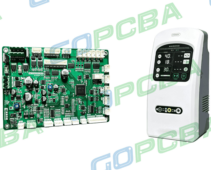
<img src="https://www.gopcba.com/wp-content/uploads/2026/08/pl149813980-oem_fast_turn_custom_pcb_rigid_enig_printed_circuit_board_quick_turn.webp" alt="Controller board with motor driver and thermal pad” />
The Host Interface
The interface to the host is a high-speed serial link, and it has to hold its impedance through the board, the connector and the cable. Because the drive is a removable device, the connector and its pin assignment are defined by the interface standard, and the layout has to match the standard rather than the other way round.
The signal path on the board is short, but it runs close to the motor driver and the power stages, which are switching large currents. Keeping that separation is the main layout challenge on the board, and the mixed-signal layout rules apply directly: separate the return currents, keep the high-speed differential pair referenced to a continuous plane, and do not allow the power return to share a path with the interface return.
The Read and Write Signal Path
The signal from the read head is very small and arrives at the preamplifier, which is usually mounted inside the drive rather than on the controller board. The connection between the preamplifier and the read channel therefore crosses the housing, and that link carries a low-level, high-bandwidth signal through a noisy mechanical environment.
That is why the interface is differential and why its impedance is controlled. The board side of the link should be laid out as a matched pair with a continuous reference, and the transition through the housing should preserve the pair geometry. Any asymmetry in that path appears as common-mode noise, which the read channel then has to reject. Signal integrity through this link is therefore maintained by geometry rather than by filtering: the pair is matched, referenced and kept short, and the surrounding layout is arranged so that the switching currents of the motor do not share its return.
Thermal Design Inside a Sealed Enclosure
The controller board sits against the drive base casting, and that casting is both the mechanical structure and the heatsink. The system-on-chip and the motor driver are the heat sources, and the heat leaves through the board into the casting, which is why the board is mounted with a thermal interface material and why the copper areas under the hot devices are large.
A thermal pad or a copper island under the package is the usual arrangement, connected to the ground plane with an array of thermal vias so that heat can spread through the board. The quality characteristics of a well-designed board include the thermal path as a first-class layout feature rather than an afterthought, and on a sealed enclosure with no airflow that path is the only route the heat has.
Failure Modes and Repair
The controller board is often the part of a drive that fails first, because it carries the power conversion and the connector that the user handles repeatedly. The common failures are the protection devices, the connector itself and the power stage, all of which sit outside the sealed housing and are exposed to electrostatic discharge and mechanical stress.
Repair of a hard disk PCB is limited by the fact that modern drives store calibration data on the board. A replacement board has to carry the same data or the drive will not initialise, which is why a board swap is not a general repair technique. That constraint shapes the design in two ways: it makes the on-board memory critical to the drive’s identity, and it pushes the design toward protecting that memory against supply disturbances.
Design Rules for a Drive Controller Board
Keep the high-speed interface pair matched and referenced, and route it away from the motor driver. Give the motor driver and the supply path the copper they need, and place their decoupling so the switching loops are small. Provide a thermal path from every power device into the casting. Protect the connector with the components that the interface standard requires, placed at the pins rather than further inside the board.
Mechanically, the board has to align with the drive housing to a tolerance that lets the flex connections reach their landing areas without strain. That makes the outline and the mounting holes part of the electrical design, since a board that stresses the flex will fail at the flex rather than at any of the components.
FAQ
Can the PCB from one drive be used in another? Not in general. The board carries calibration and configuration data that is specific to the mechanical assembly, so a replacement has to have that data transferred. Without it the drive will not spin up correctly even though the board is electrically sound.
Why does the connector fail so often? Because it is the part the user handles, it is exposed to electrostatic discharge, and it carries the host signals through a mechanical interface that is inserted and removed repeatedly. Placing the protection devices at the connector is what limits the damage.
Does the board carry the only copy of the drive firmware? It carries part of it, along with the configuration data. The firmware itself is usually split between the board and the platters, which is why both have to match for a drive to function after a repair.