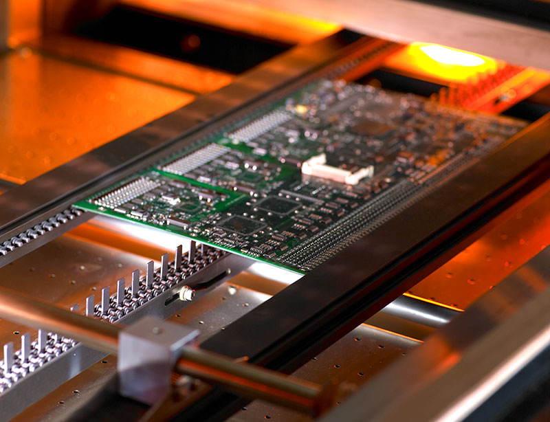
Copper Inlay PCB: Embedded Copper for High-Power Thermal Management
Copper inlay PCB technology places a solid copper block inside a cavity machined into the laminate, so heat from a power device travels into metal rather than through resin. Copper conducts at roughly 400 W/m·K while a typical FR-4 dielectric manages only 0.2 to 0.4 W/m·K. When a design has to remove several watts from a footprint smaller than a thumbnail, that difference in thermal conductivity decides whether the junction stays inside its rating.
Why Copper Inlay PCB Construction Exists
Most thermal vias help by moving heat vertically through a thin dielectric, but a via barrel is a small cross section filled with plated copper of limited thickness. A copper inlay replaces the dielectric under the heat source with bulk metal, which spreads heat laterally before it enters the rest of the board. The result is a much lower local thermal resistance and a flatter temperature profile across the component footprint.
Heat spreading also matters for neighbouring parts. If a hot spot is left to soak into the laminate, nearby passives, solder joints and electrolytic capacitors all run hotter than they should. A large metal pad under the source lowers the peak temperature and keeps the gradient across the assembly gentle.
How a Copper Inlay PCB Is Built
The process starts with an engineering review. The fabricator studies the placement of the block, the depth of the cavity, the final board thickness and the layer count to confirm that pressing, drilling and plating can all be done without deforming the panel. Design rule conflicts are far cheaper to fix at this stage than after lamination, so it helps to follow manufacturable design guidelines from the first revision.
The copper block is then machined to size, and the cavity is routed or milled into the prepreg and core stack. Positioning features such as dowel holes or alignment marks keep the insert square to the circuit pattern. During layup the block sits in the cavity and the stack is pressed, so resin has to flow around the insert and fill every gap without trapping air.
After pressing, the panel is drilled, plated and imaged like any multilayer board. Surface finish follows, and the part is inspected for voids, delamination and copper-to-copper registration before electrical test.
Materials: FR-4 and High-Tg Laminates
Standard FR-4 remains the most common base material for embedded copper boards because the insert carries the thermal load and the laminate mainly has to survive processing. For products that operate in hot environments, a high-Tg FR-4 raises the glass transition temperature and keeps the resin stiffer at elevated temperature, which reduces movement around the cavity. Where signal integrity is demanding, a low-loss material can be substituted, though the pressing window becomes narrower.
Resin choice also controls how well the cavity fills. A resin-rich prepreg flows more easily around a block, and it also shrinks more during cure. Materials with a higher filler content resist shrinkage and improve dimensional stability at the cost of flow.
Copper Thickness and Cavity Tolerance
Insert thickness is usually matched to the stack so the block sits flush with, or slightly below, the copper surface. A projection of more than about 50 µm creates assembly problems, while a recess deeper than about 100 µm can trap paste and starve the solder joint. Cavity width tolerances of ±0.1 mm are realistic in volume production, and tighter values should be discussed case by case.
Copper plugs are available in several thicknesses. Thicker metal spreads heat further but adds mass and cost, so the right value is the one that keeps the hottest junction under its limit without turning the assembly into a heat sink.
Thermal Simulation and Heat Spreading
Before committing to an inlay, model the board with the real power map. A steady-state simulation using the actual copper area, via field and airflow will show whether the insert is needed at all, or whether a dense array of thermal vias under the pad is enough. Many hot designs turn out to be limited by copper area rather than by dielectric resistance.
When the insert is justified, use the simulation to choose its footprint. Extending the block a few millimetres beyond the device outline usually costs little and lowers spreading resistance noticeably, because heat leaves the metal into the surrounding plane through a longer perimeter.
CTE Mismatch and Laminate Stress
Copper expands at about 17 ppm/°C while FR-4 in the X-Y plane is closer to 14 to 16 ppm/°C, and the difference grows sharply above Tg in the Z axis. A large block restrained by resin therefore loads the laminate on every thermal cycle. The risk is highest at the cavity corners, where stress concentrates and delamination begins.
Practical countermeasures include rounding the block corners, keeping the insert as small as the thermal budget allows, and avoiding a stack that places the block against a thin dielectric layer. For harsh environments, thermal cycling between -40 °C and +125 °C shows whether the design has margin.
Voids, Misregistration and Delamination
Trapped air around the insert appears as voids after lamination, and a void blocks heat as effectively as the resin it replaced. Voids usually come from insufficient resin flow, a poor block fit or a pressing profile that cures the resin before it has filled the cavity. Slower ramp rates and a slight resin excess solve most cases.
Misregistration is a placement issue: if the block shifts, the copper pad above it no longer lands where the stencil expects. Delamination is a stress issue and shows up after reflow or thermal cycling rather than at incoming inspection, which is why cross-sectioning a sample from each lot is worth the cost. Moisture protection such as potting and dispensing adhesives can extend life in condensing environments but will not repair a weak bond line.
Electrical Clearance and Voltage Isolation
A metal insert is a conductive body at some potential, so creepage and clearance to surrounding copper must be checked with the same discipline as any other net. On high-voltage designs, keep the cavity wall thick enough to meet the applicable isolation requirement, and remember that the insert can become the shortest path to the chassis if mounting hardware touches it.
Where the block carries current as well as heat, size the connection with the same trace width and current calculation used elsewhere on the board, and avoid necking the copper down at the cavity edge.
Where Copper Inlay Boards Are Used
Typical applications include motor drives, LED lighting engines, power conversion stages, laser drivers and RF power amplifiers. In each case a small number of components dissipate a large share of the total power, so local thermal management pays for itself. Boards that spread heat evenly across the surface rarely need an insert.

Cost is the other side of the trade. The cavity, the machined block, the extra lamination control and the added inspection all raise the price compared with a plain multilayer board, so the decision should be justified by a measured temperature problem rather than by habit. Reviews at gopcb normally start with the thermal map, the insert geometry and the cavity tolerance, because those three inputs decide whether the rest of the stack is manufacturable.
FAQ
Does a copper inlay PCB always beat a heavy copper board? Not always. Thick plated copper spreads heat over a wider area and costs less, but it cannot match the through-thickness conductivity of bulk metal under a small die. Inlays win when the heat source is concentrated and the board area is limited.
Can an inlay be combined with thermal vias? Yes, and the combination is common. Vias move heat from the component pad into the insert, and the insert then spreads it laterally into the ground planes. The via field should be dense under the die but open enough to leave room for resin flow.
What should be specified when requesting a quote? Provide the layout, the final board thickness, the insert dimensions and thickness, the cavity tolerance, the surface finish and the expected thermal cycle range. A cross-section drawing of the intended stack removes most of the ambiguity.