ENIG PCB: Immersion Gold Thickness and Black Pad Control
An ENIG PCB uses electroless nickel followed by immersion gold to protect copper pads. The nickel layer does the real work: it is a hard, solderable barrier that stops copper from diffusing into the joint, while the gold layer is only tens of nanometres thick and exists to keep the nickel from oxidising before assembly. The finish is flat, which is why it dominates fine pitch and ball grid array designs.
What the Finish Actually Is
Electroless nickel plating is autocatalytic. The copper pad is catalysed, then a reducing agent in the bath, usually sodium hypophosphite, converts nickel ions into a nickel-phosphorus alloy on the surface. Because no current is applied, the deposit covers isolated pads, thin traces and dense arrays evenly, and the resulting nickel-phosphorus layer is harder than pure nickel.
Immersion gold then deposits by a displacement reaction. Gold ions in solution take electrons from the nickel and plate out, while a small amount of nickel dissolves into the bath. That mechanism is self-limiting: once the surface is covered, the reaction stops, which is why immersion gold is thin and never builds to a measurable thickness the way plating does.
Nickel Thickness and Immersion Gold Thickness
The nickel thickness in commercial work is normally 3 to 6 µm, with roughly 4 to 5 µm being the common target. Thinner nickel risks a porous barrier that lets copper diffuse through during reflow; much thicker nickel adds stress and cost without improving solderability. Phosphorus content usually falls between 7 and 10 percent in the mid-phosphorus bath that most fabricators run.
Gold is typically 0.05 to 0.20 µm. Below about 0.05 µm the coverage becomes patchy and the nickel can oxidise, while above roughly 0.20 µm the extra gold embrittles joints and increases the risk of the corrosion known as black pad. Fine pitch devices and wire bonding applications sometimes need the thicker end of the range, which is why the specification should always name a tolerance band rather than a single value.
Black Pad: Causes and Detection
Black pad is a corrosion of the nickel surface that happens during the immersion gold step. If the bath is over-active, the temperature is too high or the immersion time is too long, the displacement reaction keeps attacking nickel after the gold has covered the pad. The result is a dark, phosphorus-rich, brittle layer with almost no solderability.
Joints made on a black pad surface look acceptable under optical inspection and fail later. The fracture is a flat, brittle break at the nickel-gold interface, which is why dye and pry testing, cross sectioning and scanning electron microscopy are used when the failure mode is suspected. Controlling bath chemistry, keeping the gold thickness low and limiting the number of reflow cycles are the practical countermeasures.
ENIG PCB Surface for BGA and Fine Pitch
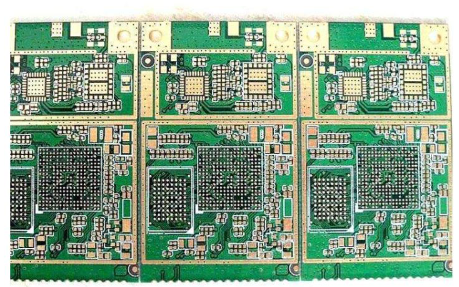
Coplanarity is the reason ENIG is chosen for area array packages. Hot air solder levelling leaves a domed solder coating that can vary tens of micrometres across a pad, which is difficult to print paste onto at a 0.4 mm pitch. ENIG is essentially planar, so stencil apertures, paste volumes and stand-off heights behave predictably.
Via-in-pad designs benefit from the same flatness, because the via must be filled and capped before the finish is applied. The combination is discussed in the note on via in pad versus plated through construction, where filling quality and finish choice are evaluated together.

Solder Joint Reliability
A well made ENIG surface produces joints that are at least as strong as those on other finishes, provided the gold stays thin. During reflow the gold dissolves into the solder and forms brittle intermetallic compounds; keeping the layer to a fraction of a micrometre means the compounds stay sparse and dispersed. This is the main reason a thicker gold layer is not automatically better.
Joint reliability also depends on the nickel-phosphorus microstructure. A consistent, mid-phosphorus deposit resists corrosion and keeps the interface uniform, while a low-phosphorus deposit is more prone to the galvanic attack that starts black pad.
Lead-Free Soldering Behaviour
ENIG is one of the most forgiving finishes for lead-free soldering. The finish tolerates peak reflow temperatures near 245 °C without degrading, and it does not consume the way an organic coating does, so a single board can pass through two or three reflow cycles plus a rework pass. Choosing between tin-lead and lead-free alloys is a separate decision covered in the comparison of lead-free versus leaded solder.
The caveat is the same as everywhere else: multiple reflows keep dissolving gold and keep growing intermetallics. If a board must survive three reflow passes, specify the lower end of the gold range.
Comparison With HASL, OSP and Immersion Silver
Hot air levelling is cheaper and gives a generous solderable coating, but it is rough and unsuitable below about a 0.5 mm pitch. OSP is the cheapest flat option, yet it survives only one reflow and has a limited shelf life. Immersion silver and immersion tin are flat and inexpensive, but silver tarnishes and can suffer creep corrosion in sulphur-bearing environments, and tin has a short storage window.
ENIG carries a higher price per square metre because the nickel and gold baths need constant analysis and the process has more steps. For designs with fine pitch, long shelf life or mixed assembly requirements, that cost is usually justified. For simple single-sided boards, it rarely is.
Storage, Handling and Specification
Gold does not oxidise, so ENIG boards store far longer than OSP or immersion tin parts. The remaining risk is contamination from fingerprints, solder resist residue and moisture, so vacuum packing with desiccant and a shelf life statement is still good practice, particularly before a second assembly operation.
A clear specification should list the nickel thickness range, the gold thickness range, the phosphorus content range, the surface finish on both sides, the resist type and the maximum number of reflows. Adding the manufacturable design guidelines from the layout review makes the documentation complete enough that the fabricator can flag a conflict before plating begins. Assembly data reviewed by gopcb follows the same structure, with the finish stack stated on the fabrication drawing so that no step is left to interpretation.
Where ENIG Fits and Where It Does Not
ENIG earns its cost on boards that mix fine pitch components with a long interval between fabrication and assembly. Industrial controllers, medical instruments, automotive modules and communication equipment all fit that description, because they often pass through more than one soldering operation and may sit in stores for months.
It is a poor match for high current terminals that must dissipate heat into a connector, for sliding or wiping contacts, and for boards where the only requirement is a cheap solderable pad on a coarse pitch. In those cases hot air levelling or an organic coating delivers the same function for less money.
Mixed finishes on one panel are common. A fabricator can mask the edge connector during ENIG and plate hard gold on the contacts, or leave part of the board with a thicker solderable coating. The layout should mark the intended finish of each region on the fabrication drawing, since ambiguity at that stage is what usually produces a rebuild.
FAQ
Is ENIG real gold? Yes, but only as a very thin layer. Typical immersion gold is 0.05 to 0.20 µm, roughly two hundred times thinner than the gold used on a jewellery item, which is why the alloy cost per board stays modest.
Can ENIG be used on gold fingers? Usually not for a connector that will be inserted repeatedly. Edge contacts need hard electrolytic gold over nickel, which is far more wear resistant than immersion gold, and the two finishes are often combined on the same panel.
Why did a joint that passed inspection fail in the field? The usual cause is a brittle nickel-gold interface from an over-active gold bath. The joint looks normal until thermal cycling opens a crack through the phosphorus-rich layer, so process control matters more than visual inspection.