Special Process PCB Selection: Heavy Copper, HDI and Rigid-Flex
Special process PCB work means going beyond the standard plated through hole multilayer build: heavier copper, laser drilled microvias, rigid-flex construction, metal core substrates, tight impedance control or cavity structures. Each of those processes adds cost and lead time, and each is worth specifying only when a real requirement cannot be met any other way. Choosing well starts with the requirement rather than with the process name.
Start With the Electrical Requirement
The first question is what the circuit has to do. Signal rate, current, isolation voltage, thermal load and mechanical form all point toward different process choices. A design that spends an hour listing processes before it lists requirements usually ends up paying for capability that the product never uses.
Write the requirements down as numbers: maximum current per conductor, allowable temperature rise, signal rise time, characteristic impedance and tolerance, board thickness, and the environmental conditions the product will see. Those values decide almost every process question that follows.
Current, Copper Weight and Thermal Path
Copper thickness is selected from current and temperature rise, not from habit. A 1 oz layer carrying 10 A over a wide plane runs far cooler than the same current in a narrow trace on a 2 oz layer, so geometry and weight have to be evaluated together. The arithmetic is covered in the guidance on trace width and current calculation.
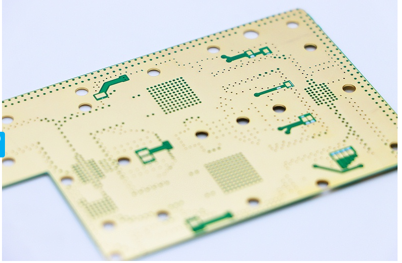
Heavy copper becomes interesting above roughly 4 oz, where the copper can also serve as a heat spreader under power devices. Beyond 6 oz the etch tolerance widens, minimum feature size grows and the price rises steeply, so the design should adopt the lowest weight that satisfies the thermal requirement. Where a single hot component drives the decision, a metal inlay or a copper coin is often a better answer than making the whole board heavier.
Routing Density and the HDI Decision
High density interconnect is justified when the escape from a fine pitch package cannot be completed on a conventional stack, or when the board area is fixed and the functional density demands more layers than fit. Below a 0.5 mm ball pitch, a microvia escape is usually the only practical route.
HDI is not a synonym for high speed. A design with a relaxed pitch and generous board area may achieve better signal integrity on a conventional eight layer stack with solid planes than on a compressed HDI build, because the reference planes are easier to keep continuous. Density and speed should be evaluated separately.
Via Structures and Sequential Lamination
Through vias are the cheapest and simplest option and should be kept wherever they do not block routing. Blind and buried vias free channels on dense boards, and the choice between them is a trade of routing area against lamination cycles. The comparison of blind and buried via structures sets out how each type affects layer count, press cycles and cost.
Every additional lamination cycle adds registration risk and extends the schedule, so an advanced via structure should be adopted only after a simpler stack has been shown to fail. Via-in-pad is a separate decision, driven by the package pitch and the need to remove through holes from the escape path.
Controlled Impedance and High Speed Constraints
If a net needs controlled impedance, the whole stack around it has to be defined: dielectric thickness, copper weight, dielectric constant after pressing and the reference plane for each layer. Single ended and differential traces need different geometry, and both should be measured on a coupon rather than assumed.
Loss and phase behaviour follow the material. Low loss laminates reduce attenuation at high frequency and keep skew under control, but they press differently and cost more. Microstrip and stripline arrangements, and the way each affects loss and crosstalk, are described in the overview of microstrip and stripline routing.
Mechanical Form and Rigid-Flex
Mechanical requirements often decide the process before electrical ones do. A board that has to bend, fit into a curved housing or survive repeated flexing calls for a flexible or rigid-flex construction with defined bend radii, coverlay openings and stiffener zones. A board that must dissipate heat into a chassis may need a metal core or an aluminium base.
Rigid-flex removes connectors and cables, which improves reliability, but it also introduces handling, folding and bonding steps that must be planned from the first layout. Bend areas should carry no plated through holes, no component pads and as few conductors as the circuit allows.
Keeping Cost Under Control
Most of the cost in a special process build comes from process steps rather than from material. Reducing the number of sequential lamination cycles, avoiding tolerances tighter than the function needs, staying with standard materials where the electrical data allows and improving panel utilisation all cut price without touching performance.
A design review before release usually finds one or two requirements that can be relaxed, and each relaxation removes a process step. Reviews at gopcb begin with the requirement list, because the cheapest way to control the price of a special process board is to stop specifying process steps that the product does not need.
Surface Finish and Solderability Requirements
Finish selection follows the assembly process. A fine pitch board that will pass through several reflow cycles needs a flat, durable finish such as one built on electroless nickel and immersion gold, while a coarse single sided board is well served by hot air levelling at a fraction of the price. Edge connectors need hard gold, and wire bonding requires a thicker gold layer than ordinary soldering.
Storage time matters as much as the first assembly. An organic coating protects the copper for only a few months and survives one reflow, so a product that sits in a warehouse before a second operation should use a metallic finish instead.
Whatever finish is chosen, it should be written on the fabrication drawing for each region of the panel, along with the thickness range. Finish ambiguity is one of the most common causes of a rebuild, because the fabricator applies what the drawing says rather than what the assembly house expected.
Documentation and the DFM Review
The last step before release is a manufacturability review. Gerber data, drill schedule, stackup drawing, impedance table, material specification, finish specification and mechanical outline should all be present and consistent. A review at that stage typically finds pad sizes below the process minimum, annular rings that are too small, or a stack that cannot be pressed flat.
Fixing those findings costs a few hours. Discovering them during fabrication costs a week and a new set of panels, which is why gopcb treats the review as a required step for every special process order rather than an optional service.
FAQ
How do I know whether my design needs HDI at all? Try to complete the escape on a conventional stack at the intended pitch. If the ball grid array cannot be routed without excessive layer count or an impractical board size, HDI is justified; otherwise it usually is not.
Is heavy copper the same as a copper inlay? No. Heavy copper increases the thickness of the whole layer, while an inlay places a solid metal block in a cavity under a specific heat source. Inlays are more effective locally and more expensive to build.
Should the special process be chosen before or after layout? The requirements should be chosen before layout and the process confirmed during the first design review, because the stack, the drill schedule and the impedance targets all depend on it.