Sputtered versus Printed Conductors on a Ceramic PCB
Ceramic substrates solve problems that FR4 cannot: they pull heat out of a device far faster, hold their dimensions at temperatures that would destroy an epoxy laminate, and lose very little energy at microwave frequencies. Once a design has settled on ceramic, the next decision is which of the two mainstream conductor technologies to use. A thin film ceramic PCB and a thick film ceramic PCB share the same alumina or aluminium nitride base, yet they are built by completely different processes and end up suited to entirely different jobs. This guide compares the two routes across conductor formation, resolution, current capacity, thermal behaviour, qualification and cost.
What the Two Technologies Have in Common
Both families begin with a sintered alumina substrate or an aluminium nitride tile. Alumina is the workhorse of the industry: ninety six percent purity grades offer roughly twenty four watts per metre kelvin of thermal conductivity, high dielectric strength and excellent mechanical stiffness at a modest price, which is why most industrial ceramic boards use it. Aluminium nitride raises thermal conductivity to between one hundred and seventy and two hundred watts per metre kelvin, and its coefficient of thermal expansion is close to that of silicon, a property that matters when a bare die is mounted directly onto the substrate.
Both routes also inherit the general advantages of ceramic. There is no glass transition temperature to design around, the dielectric constant stays stable over a wide temperature range, insulation resistance is very high, and the material resists most chemicals and radiation. Neither process uses a woven reinforcement, so there is no fibre weave to cause skew or local impedance variation across a panel. What separates the two technologies is how the conductor layer is created and how thick it ends up.
Thin Film Ceramic PCB: Vacuum Deposition and Photolithography
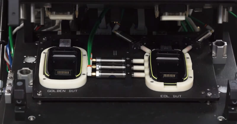
A thin film ceramic PCB is built with the tools of semiconductor manufacturing. Titanium, copper, gold or nickel layers are deposited by sputtering in a vacuum chamber, patterned by photolithography, and etched to leave conductors that are typically between one and five micrometres thick, with ten micrometres at the practical top of the range. Because the pattern is defined optically rather than printed, line width and spacing can fall below twenty five micrometres on advanced processes, and the edge of each track is clean and well defined.
The result behaves like a high density interconnect on a ceramic carrier. Fine resolution allows controlled impedance traces at microwave frequencies, tight tolerance on conductor width, and dense routing into a small die footprint. Thin film also delivers very flat surfaces and excellent run to run repeatability, which matters for filters, couplers and matching networks where a small width error becomes a frequency shift. The penalty is process cost and panel size, since vacuum equipment handles smaller substrates than a printing line.
Thick Film Ceramic PCB: Screen Printing and Sintering
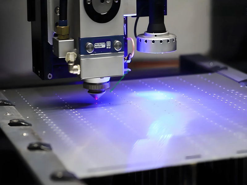
A thick film ceramic PCB is produced by printing conductive paste through a mesh screen onto the ceramic, drying it, and firing the panel at high temperature so that the metal particles sinter into a dense, adherent track. Conductors are commonly between ten and one hundred micrometres thick, far heavier than any sputtered layer, and paste systems based on silver, gold, copper or silver palladium allow the metallurgy to be matched to the assembly process and the operating environment.
Screen printing is a mature, high volume process. Tooling costs are low, panels are processed in batches, and the same sequence can be repeated for resistors, dielectric layers and crossovers alongside the wiring, so a complete passive network can be printed in one build. Its resolution limit is set by the screen mesh and the rheology of the paste, so routine minimum features sit in the hundred micrometre region, with finer lines possible only at reduced yield.
Line Width, Tolerance and Routing Density
The gap in resolution between the two processes is roughly an order of magnitude. Thin film routinely holds conductor widths and gaps in the tens of micrometres with tolerance measured in single micrometres, which supports high density interconnect geometry, flip chip escape routing and multi layer radio frequency networks inside a small area. Thick film typically works at a few hundred micrometres for both line and gap, with tolerances in the tens of micrometres after firing shrinkage is accounted for.
The practical consequence is board area, and it shows up first at the die or transducer interface. A design with many nets converging on a small component runs out of room on a printed pattern long before it runs out of thermal capacity, while a thick film build with generous geometry is far cheaper per unit area. The decision is often made simply by counting how many nets must cross a given edge of the substrate.
Current Capacity and Thermal Behaviour
Conductor thickness governs current carrying capability. A hundred micrometre silver track carries far more current than a five micrometre sputtered layer, so power modules, lamp drivers and heater circuits are natural thick film territory. Where a thin film conductor must carry significant current, the designer either widens the track, adds copper plating on top of the sputtered seed layer, or moves the function to a separate heavy copper structure on the same substrate.
Heat spreading, by contrast, depends mainly on the ceramic body rather than the metal. Aluminium nitride conducts several times better than alumina, so a power device on an AlN substrate spreads its heat over a larger area and runs cooler for the same copper pattern. Thick film pastes also tolerate higher continuous operating temperature, which suits automotive and industrial loads where the ambient is already elevated.
Where Each Technology Fits
Thin film suits applications where geometry and signal behaviour dominate the specification: microwave and millimetre wave modules, filters, couplers, high precision sensors, infrared detector arrays, laser diode carriers, and substrates that must accept a bare die with fine pitch bumps. The premium is paid for resolution and electrical repeatability rather than for power handling or raw current capacity.
Thick film suits power and harsh environment electronics: motor drives, LED modules, high temperature sensors, ignition and under bonnet circuits, heater elements and resistor networks printed in the same sequence as the wiring. It also suits programmes where a proven, inexpensive and widely available process matters more than the finest achievable line, because several suppliers can quote the same design.
Qualifying a Ceramic Build
Whichever route is chosen, the qualification plan should cover the parameters that genuinely vary in production: conductor width and gap, sheet resistance of printed resistors, dielectric withstand voltage, and adhesion after thermal cycling. For radio frequency work, add a coupon that measures insertion loss and impedance on the same panel as the product, because the electrical behaviour of the finished conductor is what the specification actually describes.
Power and thermal cycling matter more on ceramic than on FR4, because the usual failure mode is a cracked joint or a lifted conductor rather than a delamination. Suppliers with real experience in ceramic substrate materials and ceramic substrate manufacturing can advise on which conductor route matches the current and thermal profile before tooling is committed.
FAQ
Is a thin film ceramic PCB more expensive than a thick film one? Yes, generally by a wide margin, because vacuum deposition and photolithography cost far more per panel than screen printing and firing. The premium is justified whenever line resolution, impedance repeatability or die attach density decide whether the product works.
Can both technologies be combined on one substrate? They can. Printed power and heater tracks are often combined with a thin film signal layer on the same ceramic tile, which puts heavy conductors where current flows and fine geometry where signals must be routed.
Which ceramic material is used most often? Alumina dominates by volume because it is inexpensive and adequate for most industrial, sensor and LED work. Aluminium nitride is selected where higher thermal conductivity or a closer match to silicon expansion is required by the application.
Related reading: thermal substrate comparison and high temperature PCB materials.