Hyperscale Data Centre PCB: Design for High Density Systems
A data centre PCB is designed against a set of constraints that ordinary server boards do not face at the same intensity. The board has to carry very high speed serial links across a long backplane, deliver hundreds of amps at sub-one-volt rails, survive continuous operation at high inlet temperature, and be serviceable by technicians who cannot afford to take the rack down.
What Makes This Class of Board Different
The first difference is the link rate. A switch or accelerator board carries dozens of high speed serial lanes running at tens of gigabits per second, and each lane has a loss budget measured in decibels that includes the board material, the vias, the connectors and the cable. Nothing in that chain can be treated as ideal.
The second difference is the current. A processor drawing several hundred amps at a core voltage below one volt requires a power delivery network whose impedance stays below a milliohm across a wide frequency band. That is a copper and capacitance problem, and it is solved in the layout rather than in the schematic.
Laminate Selection for Long Channels
At these rates the dielectric loss of the laminate becomes the dominant term in the channel budget. A general purpose epoxy laminate contributes enough loss over a long backplane trace to close the eye at the receiver, which is why a low loss laminate is used as a matter of course rather than as an option.
The choice is made from a loss budget rather than from a material ranking. The designer calculates the reach required, subtracts the connector and cable loss, and selects the laminate that leaves enough margin at the receiver. Copper roughness matters at these rates as well, so the foil type is specified alongside the laminate, following the reasoning in FPGA board high speed interfaces.
Power Delivery at High Current
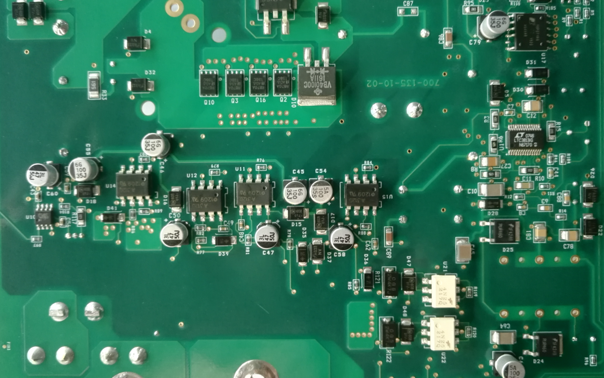
Delivering several hundred amps at a core voltage means that a hundred microohms of unintended resistance is a hundred millivolts of drop, which is a significant fraction of the total budget. The power plane is designed as a network of wide copper shapes rather than as a plane, and the current is carried by many layers in parallel through large numbers of stitching vias.
Decoupling is equally distributed. The bulk capacitance handles the slow transient, the ceramic capacitors handle the fast one, and the plane pair handles the very fast one. Placing the ceramic capacitors where their loop inductance to the load is minimal is a placement problem that dominates the layout of the processor region, and the same principles apply as in trace width and current calculation.
Signal Integrity Across Connectors
A data centre board rarely connects directly to another board; it connects through a connector, a cable or a midplane. Each of those transitions contains a discontinuity that reflects energy, and the reflections have to be kept small enough that the equaliser in the receiver can still recover the data.
The via transitions are as important as the connectors. A via stub on a thick backplane creates a resonance that can fall inside the band of interest, which is why back drilling is used on the thickest designs to remove the unused portion of the barrel. Ground return vias placed beside every signal via keep the transition impedance close to the trace impedance, as described in blind and buried via stack selection.
Thermal Design for Continuous Load
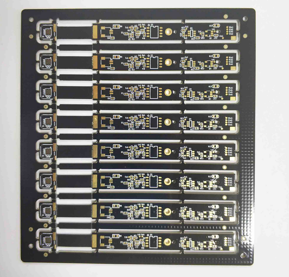
Data centre hardware runs at high utilisation continuously, so its thermal design is a steady state problem rather than a peak problem. The board is expected to conduct heat from the processor into a cold plate or into the airflow, and the copper under and around the device is the first part of that path.
The inlet temperature in a modern facility can be well above the traditional twenty degrees, which reduces the available thermal margin for every component on the board and makes the copper area under each device more important than it would be in a cooled enclosure. The board layout therefore has to keep heat sources apart, avoid placing temperature sensitive components such as crystals and optical modules in the thermal shadow of a processor, and provide a defined thermal interface at the mounting points.
Stackup and Layer Assignment
A board of this class is built from repeating units of a signal layer, a ground plane and a power plane. The repetition is deliberate, because it gives every high speed layer its own reference and keeps the return path short, and it allows the power delivery network to be distributed across many plane pairs.
Signal layers are then assigned in pairs, with the two layers of a pair routing orthogonally so that broadside coupling between them is minimized. Layer changes are planned rather than improvised, because each via costs a little loss and a little impedance discontinuity, and on a design with thousands of lanes those costs accumulate across the whole channel budget.
Mechanical Scale and Serviceability
These boards are physically large, and a large board is harder to keep flat through lamination and through the reflow cycles of assembly. Thick copper planes, a balanced stackup and sometimes a stiffener or a metal frame are used to hold flatness, because a board that warps will not seat in its connector reliably.
Serviceability constrains the layout as much as the electrical design does. Connectors and mounting hardware have to be reachable, hot components have to be replaceable without removing the board, and the labelling has to identify every cable position unambiguously. In a rack of identical units, a mislabelled cable is a maintenance error waiting to happen.
Reliability and Availability
The business case for this hardware depends on availability, and availability is measured in hours of downtime per year. That means components are derated, thermal margins are kept rather than consumed, and the failure of a fan or a power supply is expected and designed for rather than treated as an exception.
On the board, that discipline shows up as conservative current densities, generous creepage distances at higher voltages, and protection circuitry that is present on every external interface. The economics that drive a consumer product toward the cheapest possible board drive this class of hardware in the opposite direction, and the extra cost per board is small compared with the cost of a single hour of unplanned outage.
FAQ
How many layers does a data centre board use? Twenty or more is common for a switch or accelerator board, driven by the number of high speed layers required and by the power and ground planes needed to deliver the current with a low impedance.
Is back drilling always necessary? It is necessary where the board is thick and the data rate is high, because the stub resonance would otherwise fall inside the channel bandwidth. On thinner boards the stub is short enough that the effect is tolerable.
Can standard materials be used for the slower interfaces? Yes, and they usually are. The loss budget applies to each interface separately, so the control and management signals run on ordinary traces while the high speed lanes get the low loss material and the controlled geometry.