Smart Charger PCB: Design for Battery Charging Circuits
A charger board looks simple from the outside and is anything but. It has to convert an input that may range from a weak USB port to a car supply, deliver a controlled current into a battery whose voltage and temperature change constantly, terminate safely, and do all of it without overheating in a sealed plastic brick with no airflow.
The Charging Sequence
Charging a lithium cell follows a defined profile. The first phase is a controlled current, usually a fraction of the cell capacity, delivered until the terminal voltage reaches its limit. The second phase holds that voltage constant while the current tapers, and the third terminates the charge when the current falls below a threshold, or after a safety timer expires.
Each phase has its own requirements on the board. The constant current phase stresses the switching stage and the sense resistor, the constant voltage phase places a demand on the regulation loop and its reference, and termination requires an accurate measurement of a current that has become small. The layout has to serve all three.
Power Path and Switching Stage
The conversion is normally a step-down converter from an adapter or a USB source, or a step-up converter when the source voltage is below the battery. In either case the switching loop is the highest di/dt region on the board and has to be made as small as the layout allows.
The input capacitor, the switch, the return diode or synchronous switch and the output capacitor form that loop. Keeping them adjacent and keeping the return path beneath the switching node minimizes both the radiated field and the voltage spike that stresses the switch. The same reasoning that applies to any switching regulator applies here with less margin, described in radiated EMI and regulator layout.
Current Sensing and Measurement Accuracy
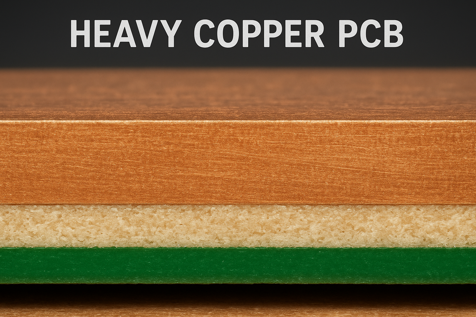
The charge current is measured across a sense resistor in the power path, and the accuracy of that measurement determines how precisely the profile can be followed. The sense resistor has to be a low temperature coefficient type, placed where it sees the average temperature of the board rather than the heat from the switching stage.
Its Kelvin connections must be taken from the inside of the pads rather than from the trace ends, or the resistance of the trace itself is added to the measurement and the error grows with current. Small as that resistance is, at several amps it produces a voltage comparable to the sense signal itself. The trace width carrying the current is set from the allowable rise, following the same calculation as any power trace.
Thermal Foldback and Protection
The charger has to reduce its current when it gets too hot, and that function is a combination of a temperature sensor, a control loop and a thermal path. The sensor has to be placed where it measures the temperature that matters, which is normally the battery or the switching device rather than the ambient.
A charging brick is often sealed with no airflow, so the board itself becomes the heat spreader. Copper area around the switching device and the sense resistor, thermal vias into any internal plane, and a defined path to the enclosure surface all contribute. Potting the assembly can help with moisture but changes the thermal behaviour, as the material choices in potting and dispensing adhesives illustrate.
Termination and Safety Logic
Termination is the point at which the product either works correctly for years or fails dangerously, and it deserves as much design attention as the conversion stage itself. A charger that continues to deliver current into a full cell will damage it, and the protection has to be independent of the main control loop. A safety timer, a second voltage limit and a temperature cut-out are the usual layers.
None of that logic is useful if the measurement it depends on is wrong, so the reference and the sense path have to be quiet. Keeping the analog measurement ground separate from the switching return and joining them at a single point is the standard approach, and the reasoning is the same as for any mixed signal design.
Cell Balancing and Multi-Cell Packs
For a multi-cell pack the board may also carry battery management circuitry, which dissipates the excess charge from the strongest cell as heat through a balancing resistor. That resistor has to be sized for the power it dissipates and placed where its heat does not reach the temperature sensors or the cells themselves.
Balancing only occurs near the end of the charge, so its contribution to the thermal load is intermittent. The layout still has to accommodate it, because the balancing resistors are often the hottest small components on the board during that phase, and their placement relative to the thermistors determines whether the temperature reading is meaningful.
Board Layout Priorities
Place the switching stage first, in the region closest to the input connector, because that is where the loop is smallest and where the heat can be spread into the largest area of copper. Keep the switching node short and fat, and keep the sense resistor immediately downstream so that the current measurement sees the same current the cell does.
The control section comes next, placed so that its ground reference does not carry the switching return. The temperature sensing and the voltage measurement connections are then routed as a quiet pair into the control region, away from the inductor and away from the output connector. Following that order avoids most of the rework that a charger board otherwise attracts.
Connectors, Cables and EMI
The output side connects to a battery through a connector and usually a short cable, and that cable is an antenna for whatever the switching stage produces. A common mode choke or a small common mode filter at the output, together with a ferrite on the cable, is often needed to pass conducted emission limits.
The input side faces the opposite problem. A USB source may be noisy or poorly regulated, and a weak adapter may collapse when the charger draws its full current. Input undervoltage detection and a soft start are therefore part of the design, and their thresholds have to be set from the worst case source rather than the typical one, following the interference control principles in mixed signal PCB design guidelines.
FAQ
Why does the charger reduce current near the end of the charge? Because holding a constant voltage while the cell approaches full would require an ever smaller current, and forcing it would overcharge the cell. The taper is a consequence of the cell chemistry, not a limitation of the circuit.
Where should the temperature sensor be placed? On the cell or on the surface closest to it, because the cell temperature is what limits the charge rate. A sensor that measures the board or the ambient will allow the cell to run hotter than intended.
Can a single chip handle the whole charge profile? Many integrated chargers do, and they are the right choice for moderate currents. Above a few amps the dissipation moves off the chip and onto external devices, and the layout becomes a power design rather than a component selection.