Alumina PCB: Material Properties and Design Guide
Alumina is the material that electronics uses when the operating temperature is too high for any polymer laminate. A board built on aluminium oxide ceramic does not soften, does not outgas and does not burn, and its thermal conductivity is many times that of FR-4. Those properties come with a completely different manufacturing process, and understanding why the processes differ explains both the cost and the design rules that follow.
Why Ceramic Rather Than Polymer
A polymer laminate is convenient because it can be laminated, drilled and plated with equipment that is widely available. Its limitation is temperature: above a few hundred degrees the resin decomposes, releasing gas and losing its mechanical properties. Ceramic does not have that limit. Alumina is stable well beyond the temperatures at which any electronic assembly operates, and its coefficient of thermal expansion is much closer to that of silicon than any polymer, which matters when a bare die is mounted directly onto the substrate.
The thermal conductivity is the other advantage. Alumina conducts heat roughly thirty times better than FR-4, so a power device mounted on a ceramic substrate has a path to the heat sink that a laminate cannot provide. That combination of thermal performance, expansion matching and high temperature stability is why ceramic appears in power modules, radio frequency circuits and sensors that operate in extreme environments. Our copper core article describes the metal based alternative for less demanding cases.
Properties That Matter in Design
The dielectric constant of alumina is around nine, which is more than twice that of FR-4. That is an advantage at microwave frequencies, because a higher dielectric constant concentrates the field and allows smaller structures, which is why ceramic is used for compact filters and couplers. It is a disadvantage for digital routing, because a given impedance requires a very narrow trace.
The dielectric strength is high, the material is chemically inert, and it does not absorb moisture at all. Those properties make it suitable for medical implants, for sensors in aggressive environments and for any application where the enclosure cannot be sealed. The mechanical behaviour is the one that catches designers out: ceramic is hard but brittle, it does not tolerate bending, and it fractures rather than deforming, so the mounting arrangement and the handling procedures both have to account for it.
Manufacturing: Co-fired and Thick Film
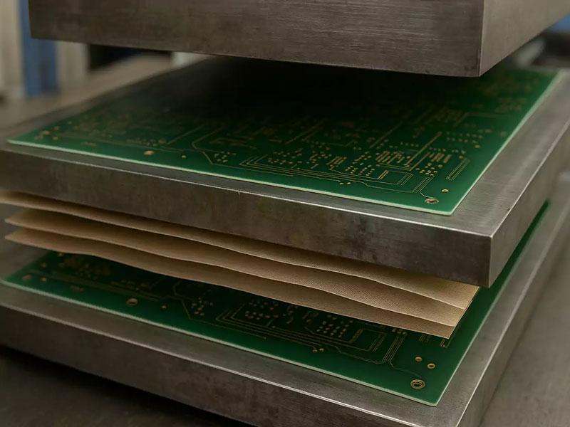
Two process families dominate. In the co-fired approach, the conductor is printed onto unfired ceramic tape using a metal paste, the tapes are stacked and laminated, and the whole assembly is fired at a temperature high enough to densify the ceramic. Firing at high temperature requires a refractory conductor, which is why tungsten and molybdenum appear in these structures, while a lower firing temperature allows copper or silver. The result is a monolithic block with internal conductors and vias, and it can be made in many layers.
In the thick film approach, the conductor is printed and fired onto an already sintered ceramic substrate, which is a much simpler process and produces a single or double sided circuit. Resistors can be printed in the same way by using a resistive paste, which is how hybrid circuits achieve their compactness. Our component tolerance and reliability notes describe how those conductors are assessed.
Design Rules and Layout Differences
Layout on ceramic follows different rules because the process is different. Vias are formed by punching the unfired tape rather than by drilling, so they are filled with conductor paste rather than plated, and the geometry of a filled via is quite different from a plated barrel. Line widths and spacing are set by the printing process rather than by etching, and the tolerances are correspondingly different.
The thermal design is also different. Because the substrate conducts heat well, heat spreads laterally through the ceramic and the design problem becomes one of getting it out of the substrate rather than of getting it into it. Where the substrate is mounted on a metal base or a heat sink, the interface between the two is usually the dominant thermal resistance, and the mechanical arrangement must keep that interface flat and free of voids.
Where Alumina Is Used
Power electronics is the largest application. A module that must switch significant current in a small volume uses a ceramic substrate to carry the heat away and to match the expansion of the silicon, and the same reasoning applies to light emitting diode arrays that are driven hard.
Radio frequency and microwave circuits use alumina because its dielectric constant allows compact structures and because its loss is low and stable. Sensor packages use it where the environment is hostile, and medical devices use it where hermeticity and biocompatibility are required. In every case the decision is driven by a requirement that a polymer laminate cannot satisfy, because the ceramic route costs substantially more and is available from far fewer suppliers.
Assembly and Handling
Assembly onto ceramic usually involves a bare die rather than a packaged component, which means wire bonding or a flip chip process, and it means the substrate has to be clean and the metallisation compatible with the bond. Solder assembly is possible where the surface is metallised appropriately, but the thermal expansion of the solder and the ceramic must be considered, and a large ceramic substrate soldered to a metal base will crack unless the joint is designed to accommodate the difference.
Handling is the other practical concern. Ceramic substrates are supplied in waffle packs or on frames, and they fracture at the slightest point load. Scoring and breaking is used to separate individual circuits, and the process is controlled far more tightly than the routing of a laminate. Our design release checklist places those checks in the review sequence.
Cost, Supply and When to Choose It
An alumina substrate costs several times what a laminate does, and the fabrication is done by a much smaller number of suppliers with longer lead times. The decision therefore comes down to whether any cheaper material can meet the requirement. If the operating temperature exceeds what a polyimide can tolerate, the answer is no. If the thermal resistance of the board is the limiting factor in the design, the answer is usually no as well, because laminating a metal core is far cheaper than co-firing ceramic.
The cases where ceramic wins are those where several requirements coincide: high temperature, thermal expansion matching to a bare die, hermeticity and sometimes radio frequency performance. A power module that must survive a thousand thermal cycles between silicon and substrate junction temperatures is the classic example, and no polymer board will do the same job regardless of how it is constructed.
FAQ
Is an alumina PCB the same as a thick film circuit? Thick film is one way of making a circuit on alumina. Co-fired ceramic is the other, and it allows many layers with internal conductors where thick film is limited to a few.
Why can copper not always be used as the conductor on ceramic? It depends on the firing temperature. A high temperature co-fired process needs a refractory metal such as tungsten, while a lower temperature process allows copper or silver.
What is the main disadvantage of ceramic substrates? Cost and brittleness. They are several times more expensive than a laminate and they fracture rather than deform, so the mechanical design and the handling procedures both have to allow for that.