PCB Solder Mask Repair: Process, Materials and Standards
Every board shop produces a small number of panels with a local defect in the solder mask: a scratch, a pinhole, a small area of exposed copper. Scrapping the panel is the safe answer and the expensive one, so the industry has developed a repair process that restores the coating locally. Done properly, it is invisible and reliable. Done badly, it produces a board that fails in the field.
What the Mask Is Protecting
The mask prevents solder from bridging between pads during assembly, keeps the copper from oxidising, provides insulation between closely spaced features and protects the surface from handling damage. It also resists the flux, the cleaning agents and the humidity that the board will meet.
A defect in the coating removes some of that protection in one place. Whether that matters depends on where it is and what it exposes. A scratch over a ground plane is cosmetic; a damaged area between two fine pitch pads is a bridging risk during assembly and a leakage path afterwards.
When Repair Is Appropriate
Repair is normally allowed on cosmetic damage and on small areas of exposed copper away from solderable features. It is generally not allowed where the defect affects the insulation over a high voltage barrier, where it changes the creepage distance or where it exposes a conductor that must remain covered for safety.
The acceptance criteria come from the applicable standard, in practice the workmanship requirements of IPC-A-600 together with the customer drawing, usually expressed in terms of the size and number of repaired areas, their location relative to pads and their distance from the board edge. Repairing a defect that exceeds the limit is a deviation, and it should be recorded as one rather than absorbed into the process.

Cleanliness and Surface Preparation
The repaired area has to be clean, dry and free of contamination, because the new material bonds to the old surface rather than to the copper. Flux residue, fingerprints and dust all reduce adhesion, and a repair that lifts later is worse than the defect it replaced.
Preparation usually involves mechanical cleaning of the immediate area and a chemical wipe, followed by a drying step. Where the damage is deep, the edges of the existing coating may be feathered so that the new material does not sit on a step. The general principles for ink behaviour apply here as much as in production, and the material characteristics are described in the discussion of solder mask ink thixotropy.
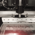
<img src="https://www.gopcba.com/wp-content/uploads/2026/08/9.png" alt="Mask touch up applied over a damaged area” />
The Repair Material
Repair materials are supplied as a two part epoxy, a single part heat cured ink or a light cured resin. They are formulated to match the colour and the finish of the production mask, and they are chosen for the curing method available at the repair station.
The colour match matters for appearance, but the mechanical match matters more. A repair material with a different expansion coefficient from the production mask will crack at the interface when the board goes through reflow, and a material with a different surface energy will affect the solderability of nearby pads if it creeps onto them.
Curing
Curing is where most repairs fail. A two part epoxy cures at room temperature over hours, a heat cured ink needs an oven cycle, and a light cured resin needs the correct wavelength and enough exposure to cure through the thickness applied.
Under-curing leaves the material soft and prone to lifting, while over-curing can discolour the mask or damage adjacent components. The cure schedule should come from the material supplier and be recorded, and where the board will be reflowed afterwards, the repaired area should be able to survive that excursion without blistering.
Verification
The repaired area is inspected visually for coverage, colour and the absence of voids, and where the repair is on a critical area, an adhesion test is performed on a sample or a coupon rather than on the production board.
A tape test at a defined adhesion level, or a scrape with a defined tool, shows whether the material has bonded. The result should be compared against the production mask rather than against an absolute figure, because the repaired area rarely matches the original perfectly and what matters is that it is good enough for the service condition. The overall set of characteristics that a board is expected to meet is described in PCB design quality characteristics.
Effect on Subsequent Assembly
A repaired board is assembled like any other, but the repaired area behaves differently under thermal load. The interface between the repair and the original coating is the weak point, and it can open during reflow, particularly if the repair material cures to a different hardness.
Repairs should therefore be positioned away from areas that see the highest thermal stress, such as the shadow of a large component, and the reflow profile should be validated on a repaired sample before the batch is released. Where the repair is near a pad, the paste deposit should be checked, because a slightly proud repair can prevent the stencil from sealing.
Prevention in Design and Process
Most mask damage is caused by handling, by rework or by the process itself. Handling marks appear where the boards are gripped, so a design that provides handling areas away from the circuitry reduces them. Rework damage is reduced by good design for rework, with space around the parts that will be replaced.
On the process side, the mask process window determines how many panels need repair. Ink viscosity, exposure energy, development and curing all affect the defect rate, and a shop that tracks repairs as a process indicator usually finds that a small change in one parameter removes most of them. The manufacturing choices that affect this are covered in PCB design guidelines for manufacturability.
Documentation and Customer Approval
Where a contract permits repair, the limit should be stated: how many repairs per board, what size, and in which areas they are prohibited. A vague requirement is interpreted differently by different operators, and a board that passes at one site may be rejected at another.
Records matter for the same reason. The location, the material and the cure schedule for each repair should be recorded against the panel, because if a fault appears later in that area the record is the only way to establish whether the repair was responsible. It also allows the repair rate to be tracked over time, which is the earliest indication of a drift in the mask process.
FAQ
Is a repaired board as reliable as an unrepaired one? For cosmetic damage in a low stress area, effectively yes. On a high voltage barrier or in a thermally stressed region, repair may not be acceptable at all.
Can the repair material be the same as the production mask? Sometimes, but the production ink needs the same exposure and development cycle, which is impractical at a repair station. Repair materials are formulated to cure by a simpler route.
How many repairs should be allowed per board? The standard will state a limit, and the answer also depends on the customer. The number should be small enough that a board with more repairs is treated as a process problem rather than a good unit.